Smart Mobility

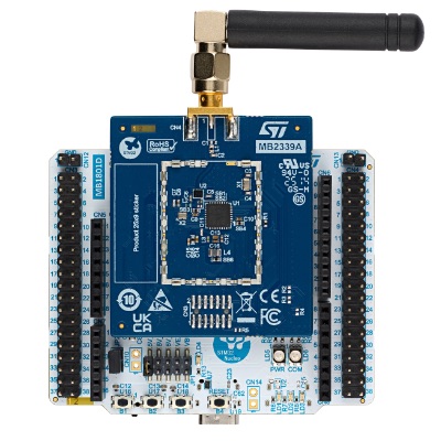
Smart BMS front-end
Smart BMS front-end
High-accuracy battery management IC with synchronized monitoring and ASIL-D ready safety features

Audio over Ethernet
Audio over Ethernet
Explore a zonal reference solution that combines synchronized audio transport, scalable integration, and simplified system design.

Power & Energy

Tailored PMICs for STM32
Tailored PMICs for STM32
Enable efficient, compact STM32 designs with STPMIC1L and STPMIC2L power management ICs.
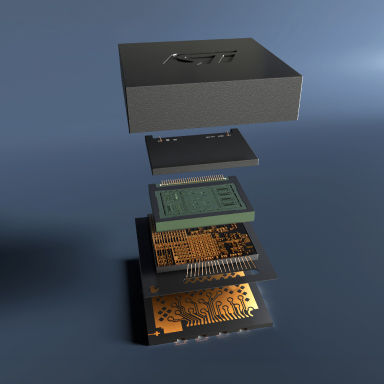
700 V PowerGaN
700 V PowerGaN
Higher switching frequencies, smaller magnetics. For datacenter power, solar conversion, EV charging, and industrial motor drives.

Cloud-connected Autonomous Things

New STM32C5 Nucleo boards
New STM32C5 Nucleo boards
Accelerate prototyping with STM32C5 Nucleo boards, designed to make development simple, flexible, and fast with Arduino and ST morpho connectivity.

Smart high-impact sensor
Smart high-impact sensor
High-g and low-g sensors with smart processing for precise, power-efficient motion tracking and impact detection.

Upcoming events
Want to know more about our latest technologies?Come and meet us.
Check out all our upcoming events Check out all our upcoming events


PCIM
Live demos and direct conversations with system experts on the latest SiC, GaN, and smart power solutions for automotive, industrial, robotics, and AI server applications. Make every watt count. Make every cycle smarter.
Tradeshow
Nuremberg, Germany 09-11 June, 2026
See our PCIM program See our PCIM program

Boost your design journey with our AI‑powered tool
Boost your design journey with our AI‑powered tool
Discover STM32 Sidekick
29 years of sustainability reporting.
Committed.14 sustainability goals.
Responsible.2027 carbon neutrality commitment.
ST annual integrated report
Our annual integrated report offers an overview of our sustainability performance in 2025 and the goals that guide our actions. We remain committed to respecting people and the planet, and to communicating transparently with our stakeholders.

Newsroom
See all the latest news from ST.
Blog
Read our latest technical articles.
Newsroom
See all the latest news from ST.
STMicroelectronics high-performance vibration sensor with in-sensor AI offers a compelling alternative to piezosensor to fast-growing industrial condition-monitoring market
STMicroelectronics raises its revenue ambition for Data Centers amidst continued strong demand for AI infrastructure

ST and quantum: bringing industrial scale to a new compute frontier

STMicroelectronics brings always-on vision to next-generation personal electronics with new ultralow-power image sensors

Blog
Read our latest technical articles.
IIS3DWB10IS, the 1st digital vibration sensor with 10 kHz bandwidth to enable new era for predictive maintenance
MASTERGAN6 and MASTERGAN7 help democratize GaN power devices thanks to integrated LDOs and new dedicated pins
PQC: Everything you wanted to know about post-quantum cryptography but were afraid to ask

Update: New STM32WL3R for remote control application now available!