The STM32 devices defined in Table 1 embed an FDCAN peripheral that supports the CAN-FD protocol according to ISO 11898-12015. Most STM32 devices support more than one instance of CAN. Refer to the product datasheet for the number of instances available on a specific device.
The range of features and functionalities offered by the Flexible Data-rate Controller Area Network (FDCAN) feature in STM32 devices is dependent on the specific implementation of the device.
To fully understand the implementation and the capabilities of the FDCAN feature, refer to the product reference manual. The rest of this document will delve deeper into the advanced functionality of the FDCAN, referred to as the FDCAN superset.
FDCAN peripheral main features
The features of the FDCAN on STM32 devices are listed below:
Compliant with CAN protocol version 2.0 part A, B and ISO 11898-1: 2015, -4
Accessible 10-Kbyte RAM memory to allocate up to 2560 words
Improved acceptance filtering
Two configurable receive FIFOs
Up to 64 dedicated receive buffers
Separate signaling on reception of high priority messages
Up to 32 dedicated transmit buffers
Configurable transmit FIFO and transmit queue
Configurable transmit event FIFO
Clock calibration unit
Transceiver delay compensation
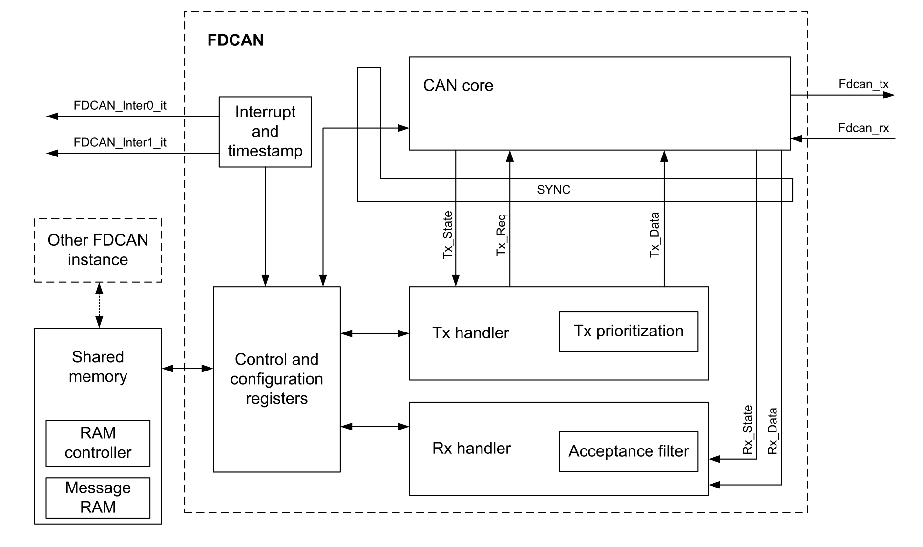
The figure below illustrates the FDCAN block diagram.
Figure 3. FDCAN block diagram
The FDCAN block diagram characteristics are listed below:
All the FDCAN instance numbers share the same memory.
Each FDCAN instance contains the CAN core.
The CAN core presents the protocol controller and receive/transmit shift registers.
The Tx handler controls the message transfer from the CAN message RAM to the CAN core.
The Rx handler controls the transfer of received messages from the CAN core to the external CAN message RAM.
RAM management
All transmitted and received messages are stored in the CAN message RAM. During CAN message RAM initialization, the user must define where to store the 11-bit filter, the 29-bit filter, the received messages and the messages to transmission.
RAM organization
The quantity of data bytes per message must be configured to determine the memory space that is required per message. The increase of the payload on CAN-FD results in more efficient memory usage and allows more messages to be stored in the allocated memory space.
A dedicated RAM reserved to FDCAN on STM32 devices is used to allocate up to 2560 words of 32 bits. This reserved RAM space makes the CPU more efficient.
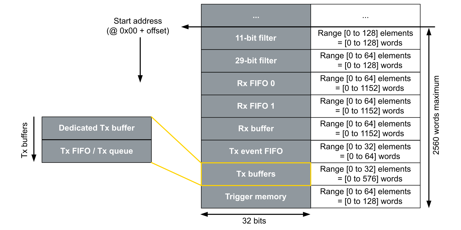
As illustrate in the figure below, the CAN message RAM is split into four different sections:
All sections of the FDCAN peripheral can be configured by the user. The sum of all elements of all sections must not be exceed the total CAN message RAM size. This RAM provides increased flexibility and performance by enabling the possibility to eliminate unused sections and to expand sufficient memory for the other sections.
The configured elements of each section are allocated in a dynamic and successive way in the CAN message RAM according to the order presented in above figure; however in order to avoid the risk of exceeding the RAM and for reliability reasons, a specific own start and end address is not assigned to each section.
FDCAN peripheral can configure three mechanisms for transmission: Tx buffer and/or Tx queue and/or Tx FIFO and can receive via Rx buffer and/or Rx FIFO. They are configured with a start-address offset and the number of memory elements to store. The starting address is predefined in the configuration (number between 0 and 2560), and it is the user’s responsibility to ensure that the number of elements per memory space does not cause them to overlap.
Note:
The reception and the transmission of a message imply the storage of an “element” at RAM level. This “element” contains only the identifier, the DLC, the control bits (ESI, XTD, RTR, BRS, FDF), the data field and the specific transmission/reception bits field for control. The remaining bits of the CAN message are handled automatically by hardware and are not saved in the RAM.
The specific bits fields for control for reception are filter index, accepted non-matching frame, and Rx timestamp. The specific bits fields for transmission are message marker and event FIFO control bit.
The number of 32-bit words allocated for each element whatever Tx buffer, Tx FIFO, Tx queue or in Rx buffer are calculated to reserve:
Header information (two reserved 32-bit-words) to allocate the identifier, the DLC field, the bits of control and the specific transmission/reception bits fields
Data (the number of 32-bit words sufficient) to contain the number of bytes per data field
The formula below determines the number of 32-bit words allocated for each element:
Element size (in words) = Header information (2 words) + Data (data field/4)
where data field is the number of data bytes per message.
Note:
If the data field is in the range of 0 to 8, 2 words are allocated for the data per element.
The necessary “element” size depending on data field range is detailed in the table below.
Table 4. “Element” size number depending on data field range
Data field (bytes)
Element size (RAM words)
0 to 8
4
12
5
16
6
20
7
24
8
32
10
48
14
64
18
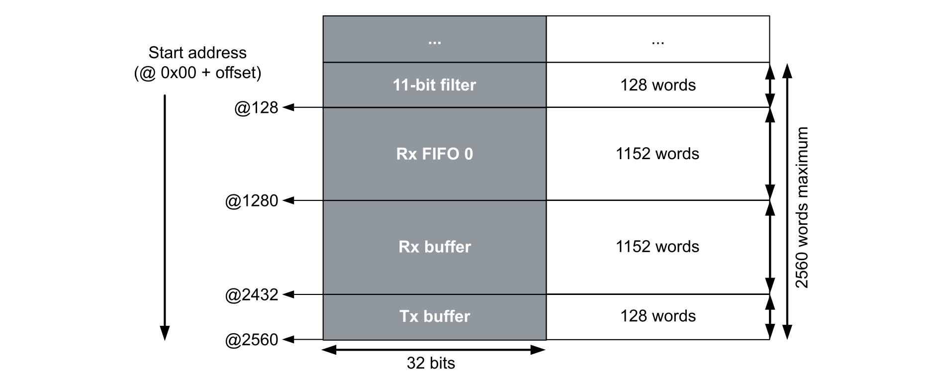
An example for efficient use of the CAN message RAM is illustrated in the figure below. This example assumes an application where the FDCAN peripheral is configured:
to send 32 messages with dedicated Tx buffer (each message contains 8 bytes in the data field)
to have 128 11-bit filters for acceptance of the messages
to receive 64 messages where each message contains 64 bytes in data field in dedicated Rx buffers
to receive 64 messages where each message contains 64 bytes in data field in Rx FIFO 0
Figure 5. RAM mapping example for and efficient use of the CAN message RAM
In this example, the allocation in the RAM is done in the following order:
Allocate 128 words in the section ID-11bits.
Reserve 1152 words for the reception of the elements in the section Rx FIFO 0.
Reserve 1152 words for the reception of the elements in the section Rx buffer.
Reserve 128 words for the elements sent in Tx buffer.
Thanks to the dynamic allocation and by not making any allocation for unused sections, the whole memory size of the RAM is used efficiently: all the 2560 words are allocated in this application.
Note:
After the configuration, the allocated address range is initialized to zero.
Multiple FDCAN instances
Most STM32 devices support more than one FDCAN instance to meet all the application requirements (refer to the product datasheet for the number of instances).
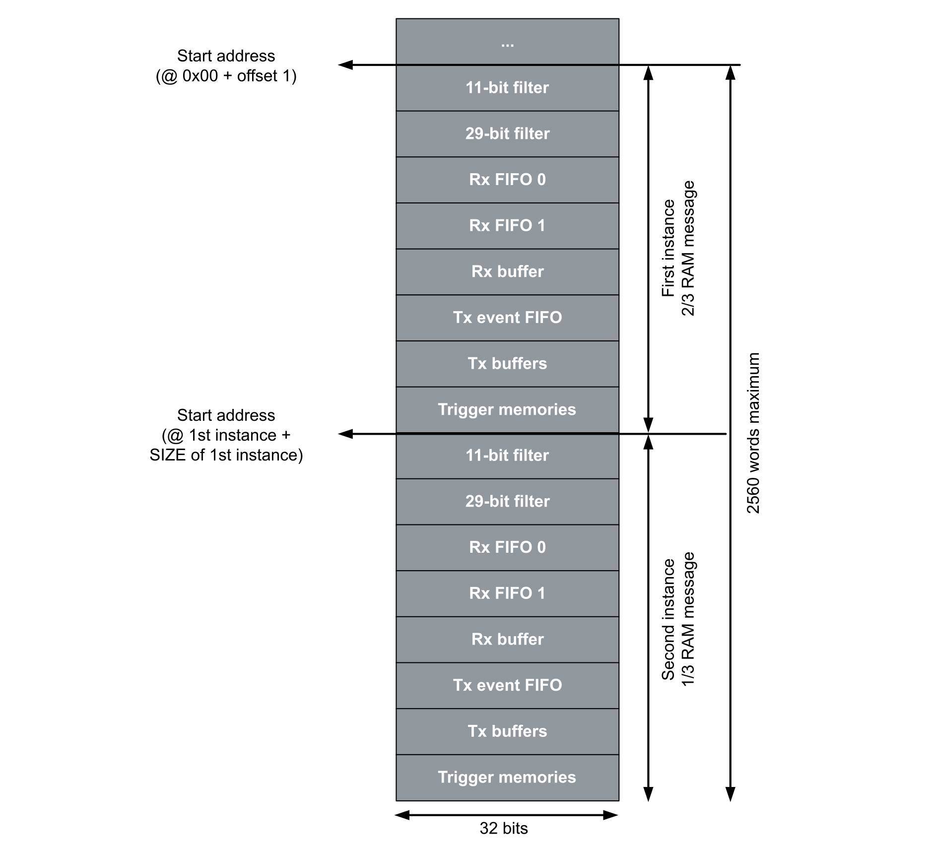
In this context, it is important to say that the RAM is shared between the different instances. The user can divide the RAM on the various instances (each instance size is chosen by indicating its start offset address).
An example of a CAN message RAM using multiple FDCAN instances is illustrated in the figure below. This example assumes that the user divides the CAN message RAM into two instances: the size of the first instance is the double of the second instance.
Figure 6. Example of CAN message RAM with multiple FDCAN instances
RAM sections
RAM filtering sections
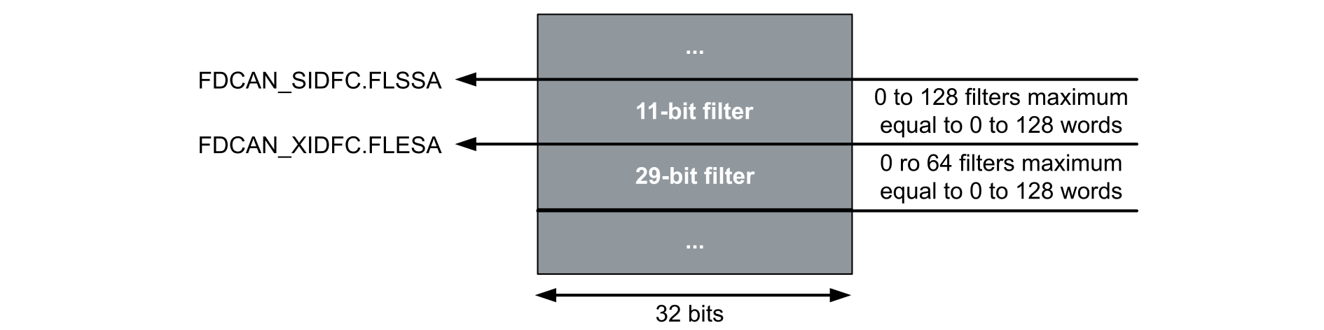
The FDCAN peripheral offers the possibility to configure two sets of acceptance filters: one for standard identifiers and one for extended identifiers to store or reject received messages. Up to 128 filter elements can be configured for 11-bit standard IDs and up to 64 filter elements can be configured for 29-bit extended IDs.
The start address of 11-bit filter section is configured via the FLSSA[13:0] bits in the FDCAN_SIDFC register and the 29-bit filter section is configured via the FLESA[13:0] in the FDCAN_XIDFC register.
The figure below shows a section of the CAN message RAM with the number of filter elements and their start addresses.
Figure 7. CAM message RAM filters section
These filters can be assigned to the Rx FIFO 0/1 or to the dedicated Rx buffers. When the FDCAN performs acceptance filtering, it always starts at filter element #0 and proceeds through the filter list to find a matching element. Acceptance filtering stops at the first matching element and the following filter elements are not evaluated for this message. Therefore, the sequence of configured filter elements has a significant impact on the performance of the filtering process.
The user chooses to enable or disable each filter element, and can configure each element for acceptance or rejection filtering. Each filter element can be configured as:
Range filter: the filter matches for all messages with an identifier in the range defined by two IDs.
Filter for dedicated IDs: the filter can be configured to match for one or two specific identifiers.
Classic bit mask filter: to match groups of identifiers by masking bits of a received identifier. The first ID configured is used as message ID filter, the second ID is used as filter mask. Each zero bit at the filter mask masks out the corresponding bit position of the configured ID filter.
Note:
If all bits equal 1, a match occurs only when the received message ID and the message ID filter are identical. If all mask bits equal 0, all message IDs match.
High-priority messages
The FDCAN can notify the user when a high priority message is received. This notifications can be used to monitor the status of incoming high-priority messages and to enable fast access to these elements.
The FDCAN detects a high-priority message with help of a message filter. A filter element provides the following settings related to high-priority messages:
Set priority and store in FIFO 0/1 if filter matches: if this message filter matches, the FDCAN informs about the high-priority message arrival and stores the element in Rx FIFO 0/1.
Set priority if filter matches: if this message filter matches, the FDCAN notifies about the high-priority message arrival but does not store the element.
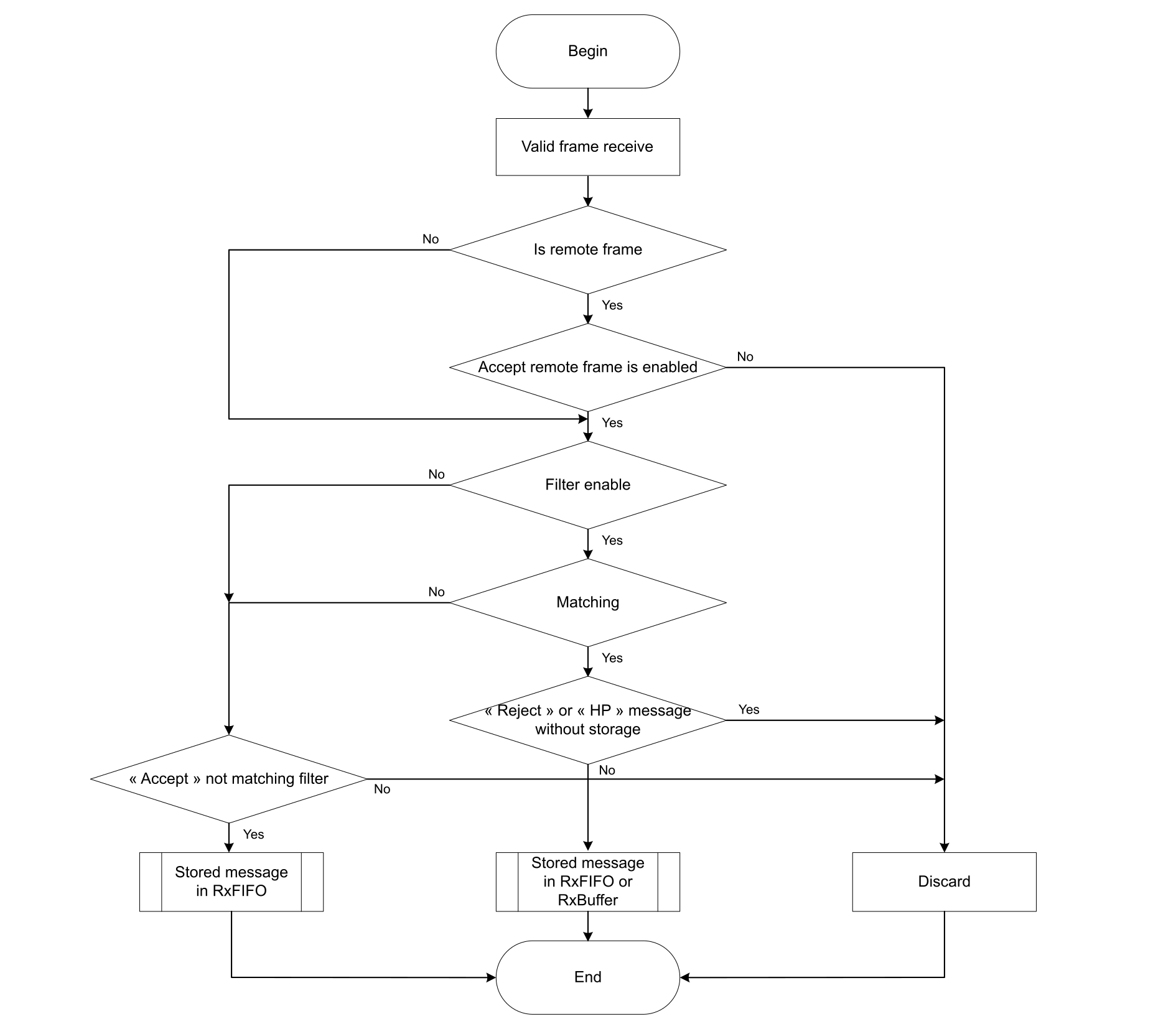
The following flow chart explains the global mechanism of an acceptance filter.
Figure 8. Global flow chart of acceptance filter
Example to illustrate the acceptance filtering
To illustrate the different types of filters that can be used and the result of each type, the assumption is that the user wants to configure the FDCAN:
to reject all the messages with identifier in the range [0x16 to 0x20]
to accept all the messages with identifier equal to 0x15 or 0x120 and to store them in FIFO 1
to accept the message with identifier equal to 0x130 and store it in the Rx buffer index 4
to accept the messages with identifier that corresponds to:
bits [10..6] = 0b111 00
bits [5..4] = don’t care
bits [3..0] = 0b00000
In this case, the filter must be configured as classic bit mask filter because the accepted identifier correspond to 0b11100XX0000 (where x can be any value in 0 or 1). The accepted identifiers are:
0b111 0000 0000 (0x700)
0b111 0001 0000 (0x710)
0b111 0010 0000 (0x720)
0b111 0011 0000 (0x730)
The base filter ID can be any value in 0x700, 0x710,0x720,0x730. The mask filter ID equals 0b111 1100 1111 (0x7CF).
The table below presents the different configurations of the standard 11-bit message ID filters, as indicated in the above example. Each standard filter element contains:
SFT bits (standard filter type)
SFEC bits (standard filter element configuration).
SFID1 bits (standard filter ID1)
SFID2 bits (standard filter ID2)
Table 5. Standard filter element configuration
Filter
Standard filter type
SFT [31:30]
Standard filter element configuration
SFEC [29:27]
Standard filter ID 1
SFID1 [26:16]
Standard filter ID 2
SFID2 [15:0]
First
00 - Range filter
011 - Reject
0x16
0x20
Second
01 - Dual ID
010 - Store in FIFO 1
0x15
0x120
Third
xx - Don't care
111 - Store in Rx buffer
0x130
0x04 (buffer index)
Fourth
10 - Classic bit mask filter
001 - Store in FIFO 0
0x700
0x7CF
The first filter is configured to reject the messages with ID in the range [0x16...0x20].
The second filter is configured to store in Rx FIFO 1, the messages with ID equal to dual ID 0x15 or 0x120.
The third filter is configured to store in Rx buffer index 4, the message with ID equal to 0x130 .
Note:
If SFEC is configured as “Store into Rx buffer” then the configuration of SFT is ignored. The acceptance filter stops at the first match. So the order of the filters is important.
This example configures the standard filters in the same way than a user can configure the extend filters (refer to product datasheet for more details).
The numerous filter possibilities of the FDCAN allow a complex message filtering in hardware, which makes software filtering redundant and saves CPU resources.
Reception section
Rx FIFO 0 and Rx FIFO 1
Two Rx FIFO can be configured in the CAN message RAM. Each Rx FIFO section can store up to 64 elements. Each element is stored in one Rx FIFO element.
The size of a Rx FIFO element can be configured via the FDCAN_RXESC register for each Rx FIFO individually. The Rx FIFO element size defines how many data field bytes of a received element can be stored. The size of an Rx FIFO element is defined by the formula specified in RAM organization.
Header information contains the identifier, DLC field, control bits and the bits fields (filter index, accepted non-matching frame, Rx timestamp).
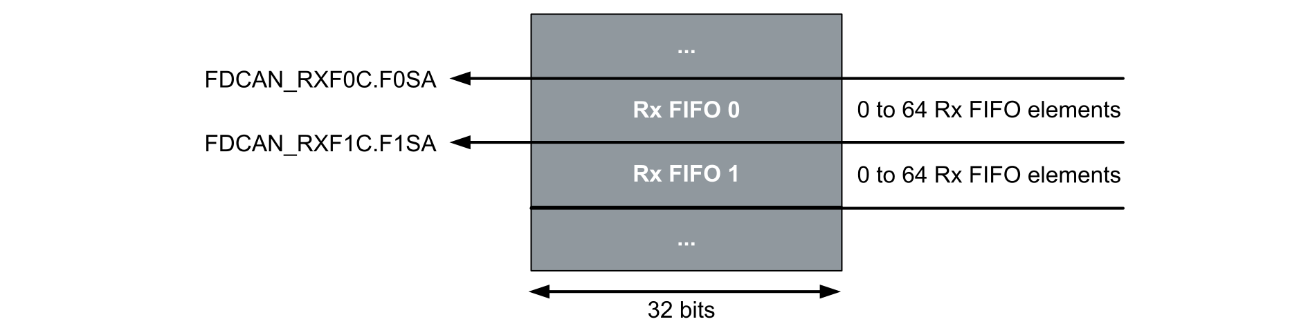
After the configuration of the element size via the F1DS[2:0] field in the FDCAN_RXESC register, the number of elements and the start address of Rx FIFO 1 must be configured respectively via the F1S[6:0] and F1SA[13:0] fields in the FDCAN_RXF1C register.
The figure below shows the Rx FIFO section on the CAN message RAM with the number of elements that can supported and the start address for each section.
Figure 9. Rx FIFO section in CAN message RAM
The start address of an Rx FIFO is the address of the first word of the first Rx FIFO element. Received elements that pass the acceptance filtering are stored in the appropriate Rx FIFO based on the matching filter element.
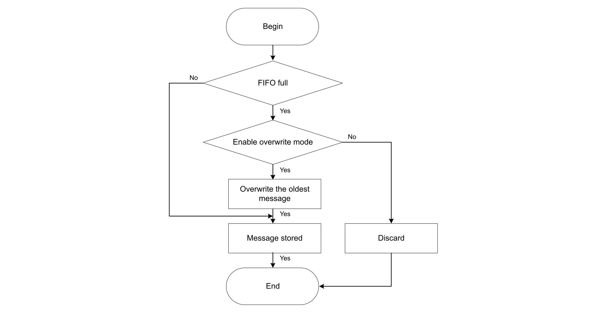
If the Rx FIFO is full, the newly arriving element can be handled according to two different modes:
Blocking mode: this is the default operation mode of the Rx FIFO, no further elements are written to the Rx FIFO until at least one element has been read out.
Overwrite mode: The new element accepted in the Rx FIFO overwrites the oldest element in the Rx FIFO and the put and get index of the FIFO are incremented by one.
To read an element from an Rx FIFO, the CPU has to perform the following steps:
Read the register FDCAN_RXF1S to know the status of the Rx FIFO.
Calculate the address of the oldest element in the RAM as with the following formula:
Oldest element address = CAN_message_RAM_base_address + FDCAN_RXF1C.F1SA (start address) + FDCAN_RXF1S.F1GI (get Index) x Rx FIFO_element_size.
Read the element from the calculated address.
After the CPU has read an element or a sequence of elements from the Rx FIFO, it must acknowledge the read. After acknowledgement, the FDCAN can reuse the corresponding Rx FIFO buffer for a new element. To acknowledge one or more elements, the CPU must write the buffer index of the last element read from Rx FIFO to FDCAN_RXF1A register. As a consequence, the FDCAN updates the FIFO fill level and the get index.
The following chart presents a simplified operation of Rx FIFO.
Figure 10. Simplified operation of Rx FIFO
Note:
The registers of Rx FIFO 0 and Rx FIFO 1 have identical registers with meaningful names by changing the number of FIFO each time.
Dedicated Rx buffer section
The FDCAN supports up to 64 dedicated Rx buffers. Each dedicated Rx buffer can store one element.
The size of a dedicated Rx buffer can be configured via the FDCAN_RXESC register. The Rx buffer size defines how many data field bytes of a received element can be stored. The size of a dedicated Rx buffer is defined by the formula described in RAM organization.
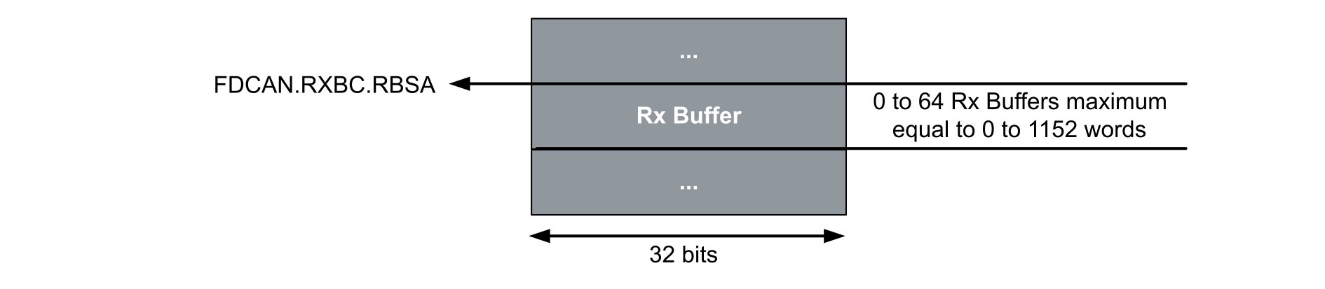
After the configuration of the element size via the RBDS[2:0] field in the FDCAN_RXESC register, the start address must be configured via the RBSA[13:0] field in the FDCAN_RXBC register.
The figure below shows the Rx buffer section on the CAN message RAM with the maximum number of dedicated Rx buffer elements that can be supported and the start address.
Figure 11. Rx buffer section on CAN message RAM
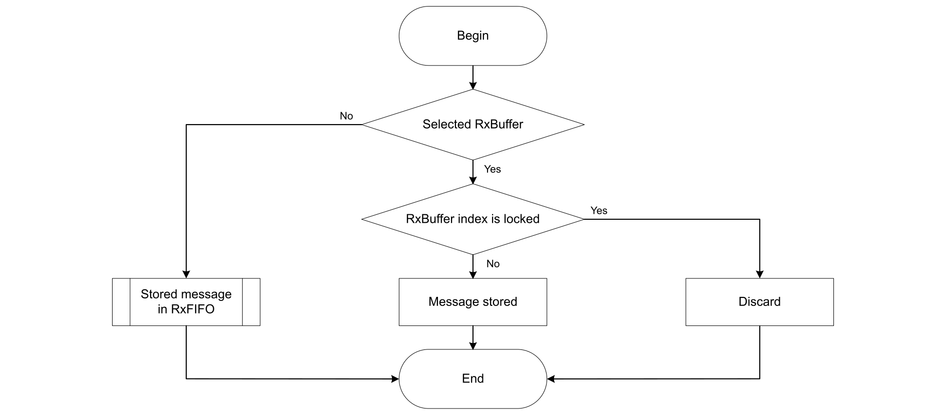
When an element is stored in a dedicated Rx buffer, the FDCAN sets the interrupt flag via the DRX bit in the FDCAN_IR register and the corresponding bit in the new data flag FDCAN_NDAT1 or FDCAN_NDAT2 registers. When bits are set in FDCAN_NDAT1/2, the respective Rx buffer is locked (not overwritten by a new element) and the corresponding filter does not match. After reading the element, the CPU has to reset the corresponding bit in FDCAN_NDAT1/2, in order to unlock the respective Rx buffer.
To read an element from a dedicated Rx buffer, the CPU must perform the following steps:
Check the bits in FDCAN_NDAT1/2 to know if a new element arrived in a dedicated Rx buffer.
Calculate the address of the element in the CAN message RAM, as determined by the formula below:
Reference Rx buffer address = CAN_message_RAM_base_address + FDCAN_RXBC.RBSA (start address) + dedicated Rx buffer index x Rx_Buffer_element_size.
Read the message from the calculated address.
The filter element can reference Rx buffers index (0 to 63) as destination for a received element. If the corresponding filter matches, the FDCAN only performs a write to a referenced Rx buffer location. In other words, the FDCAN does not write to unreferenced Rx buffer locations.
Example for the relative configuration of Rx buffer number to the Rx buffer index
In order to configure a filter element to reference an Rx buffer index 60, at least 61 Rx buffers must be configured.
Note:
The user must choose the best configuration to avoid wasting the RAM.
The figure below presents a flowchart to simplify the operation of Rx buffer.
Figure 12. Simplified operation of Rx buffer
Differences between dedicated Rx buffer and Rx FIFO
As presented in the previous section, the FDCAN has two mechanisms: either a dedicated Rx buffer or Rx FIFO 0/1 can be configured to store a received element.
The differences between a dedicated Rx buffer and an Rx FIFO are described in the table below.
Table 6. Differences between dedicated Rx buffer and Rx FIFO
Feature
Dedicated Rx buffer
Rx FIFO
Sections to configure
64 dedicated Rx buffers can be configured .
Two Rx FIFO can be configured.
Elements per section
Configured to contain only one element per buffer
May contain one or more elements (up to 64 elements) per section
Position in the RAM
The user chooses the buffer index.
The position in the RAM is automatically and dynamically managed (using the incrementing of get/put index).
Discards newly arriving element configuration
Discards the newly arriving element when buffer is locked.
Note: The user must reset the corresponding bit in FDCAN_NDAT1/2.
Discards the newly arriving element when Rx FIFO is full (blocking mode by default).
Note: Overwrite mode option to receive the new element and overwrite the oldest element.
Transmission section
Tx event FIFO section
By using a Tx event FIFO, the CPU gets the following information about the sent elements:
in which order the elements were transmitted
the local time when the frame was transmitted for each element
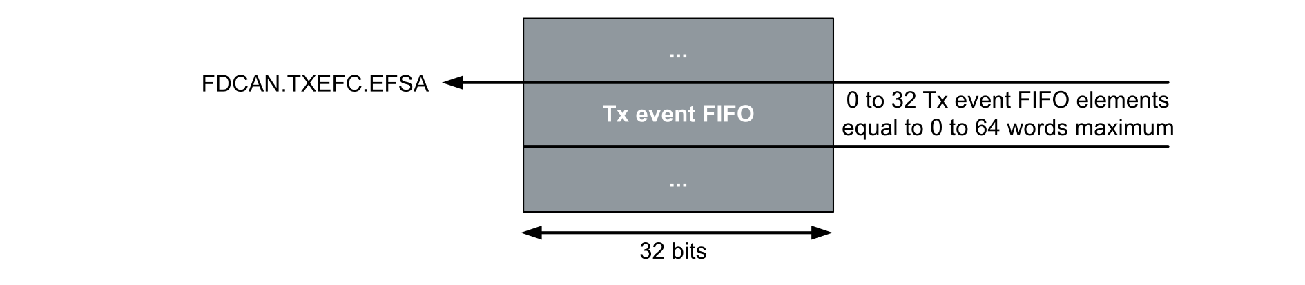
The FDCAN provides a Tx event FIFO. The use of this Tx event FIFO is optional. After the FDCAN successfully transmitted an element on the CAN bus, it can store the message ID and the timestamp in a Tx event FIFO element. A Tx event FIFO element is a data structure that stores information about transmitted messages. The Tx event FIFO can be configured via the FDCAN_TXEFC register (Tx event FIFO configuration). The FIFO can store a maximum of up to 32 elements.
The following figure shows an example of a CAN message RAM where the Tx event FIFO elements are stored and the EFSA[13:0] field contains the start address.
Figure 13. Tx event FIFO section in the CAN message RAM
The address of a Tx event FIFO element in the CAN message RAM, is determined by the formula below:
Tx event FIFO element address = CAN_message_RAM_base_address + FDCAN_TXEFC.EFSA (start address) + FDCAN_TXEFS.EFGI (get index) x Tx_event_FIFO_element_size
To link a Tx event to a Tx event FIFO element, the message marker from the transmitted Tx buffer is copied into the Tx event FIFO element.
Events are stored in Tx event FIFO only if the EFC bit (store Tx events) in the Tx buffer element, equals 1.
When the Tx event FIFO is full, no further elements are written to the Tx event FIFO until at least one element is read out and the Tx event FIFO get index is incremented. If a Tx event occurs while the Tx event FIFO is full, this event is discarded. To avoid a Tx event FIFO overflow, the Tx event FIFO watermark can be used.
After the CPU read an element or a sequence of elements from the Tx event FIFO, the CPU must acknowledge the read. Therefore, it writes the index of the last element read from Tx event FIFO via the EFAI[4:0] field in the FDCAN_TXEFA register.
Tx buffer section
For a module to transmit an element, the element is formed within the defined memory space and the transmission is initiated. The transmitted elements are stored in the Tx buffer section where the user can choose the mechanism to be used: a dedicated Tx buffer and/or Tx queue or Tx FIFO.
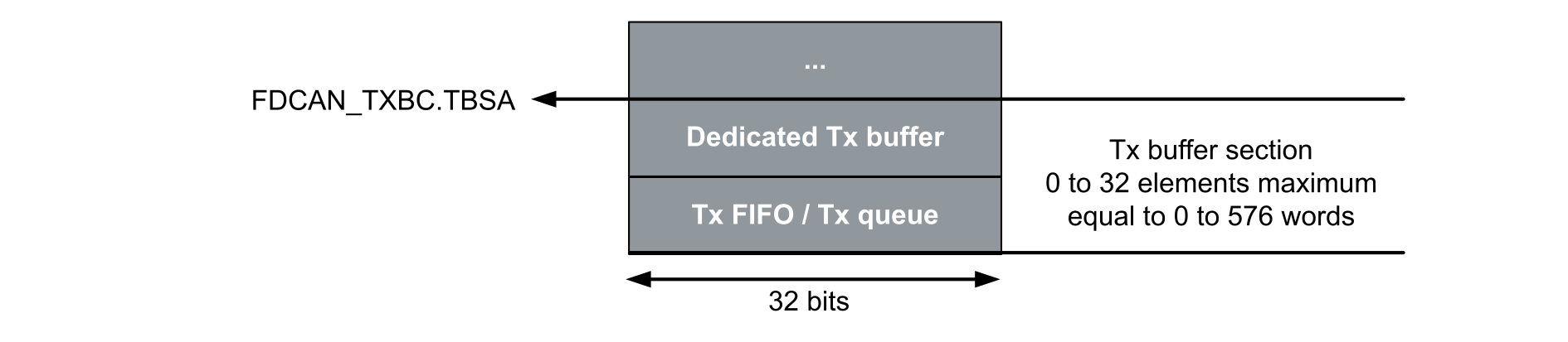
Up to 32 elements are supported by the FDCAN. Each element stores the identifier, the DLC, the control bits (ESI, XTD, RTR, BRS, FDF), the data field, the bits field message marker and the event FIFO control bit of only one message.
The allocation on the RAM is done in the following order: if dedicated Tx buffers are used by the application, then they are allocated before the Tx FIFO and Tx queue. The user can choose only Tx queue or Tx FIFO in the same application: a combination of them is not supported by the FDCAN.
As indicated in the figure below, the start address of Tx buffer section is configured via the TBSA[13:0] field in the FDCAN_TXBC register.Figure 14. Tx buffer section in CAN message RAM
Note:
As indicated in the previous section, the allocation in the RAM is made in a dynamic and successive way so if the user does not configure a dedicated Tx buffer mechanism. The Tx buffer section contains only the configured Tx queue or Tx FIFO and it is stored in the start section address.
Dedicated Tx buffers
The number of dedicated Tx buffers are configured via the NTDB[5:0] field in the FDCAN_TXBC register. Each dedicated Tx buffer is configured with a specific identifier to store only one element. The transmission is requested by an add request via the FDCAN_TXBAR register. The requested messages arbitrate externally with messages on the CAN bus, and are sent out according to the lowest identifier (highest priority).
The memory requirements for the dedicated Tx buffers depend on the Tx buffer element size. The Tx buffer element size defines the number of data bytes belonging to a Tx buffer.
The address of a dedicated Tx buffer in the CAN message RAM is calculated using the formula below:
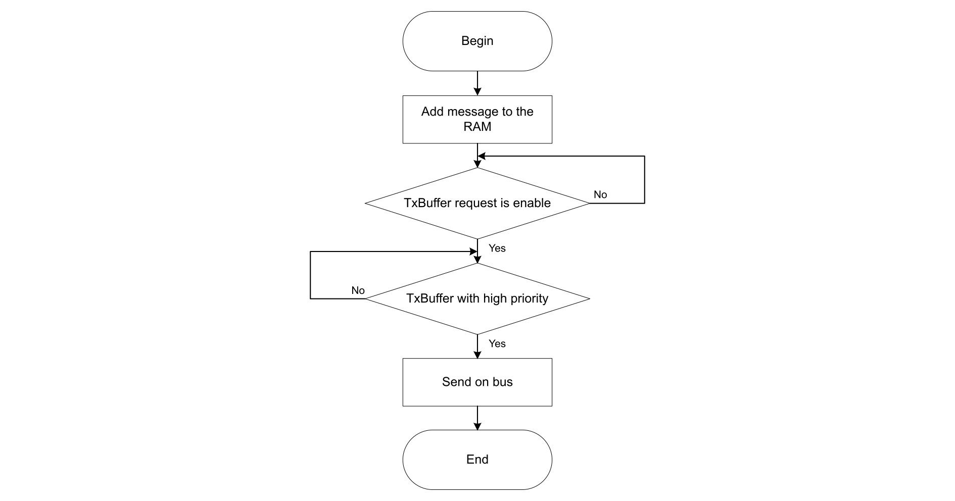
The following flow chart is used to simplify the operation of a transmission with the Tx buffer mechanism.
Figure 15. Transmission with Tx buffer mechanism
Note:
If multiple dedicated Tx buffers are configured with the same ID, the Tx buffer with the first transmission request is transmitted first.
Tx FIFO
The Tx FIFO operation is configured by writing 0 to the TFQM bit in FDCAN_TXBC. The elements stored in the Tx FIFO are transmitted starting with the element referenced by the get index via the TFG1[4:0] field in FDCAN_TXFQS. After each transmission, the get index is incremented cyclically until the Tx FIFO buffer is empty.
The Tx FIFO enables the transmission of elements in the order these elements have been written to the Tx FIFO. The transmission is independent of the priority of the respective identifiers because the first/oldest element in the FIFO is sent out first.
The FDCAN calculates the Tx FIFO buffer free level via the TFFL[5:0] field in FDCAN_TXFQS as a difference between get and put index (get and set index two mechanism increments each transaction to indicate the next buffer position on the RAM to read or write element). This value indicates the number of available (free) Tx FIFO elements.
New transmit elements must be written to the Tx FIFO starting with the Tx buffer referenced by the put index indicated via the TFAQPI[4:0] field in FDCAN_TXFQS.
The address of the next free Tx FIFO buffer in the CAN message RAM is calculated with the below formula:
Next free Tx FIFO buffer address = CAN_message_RAM_base_address + FDCAN_TXBC.TBSA (start address) + FDCAN_TXFQS.TFQPI (put Index) x Tx_FIFO_element_size
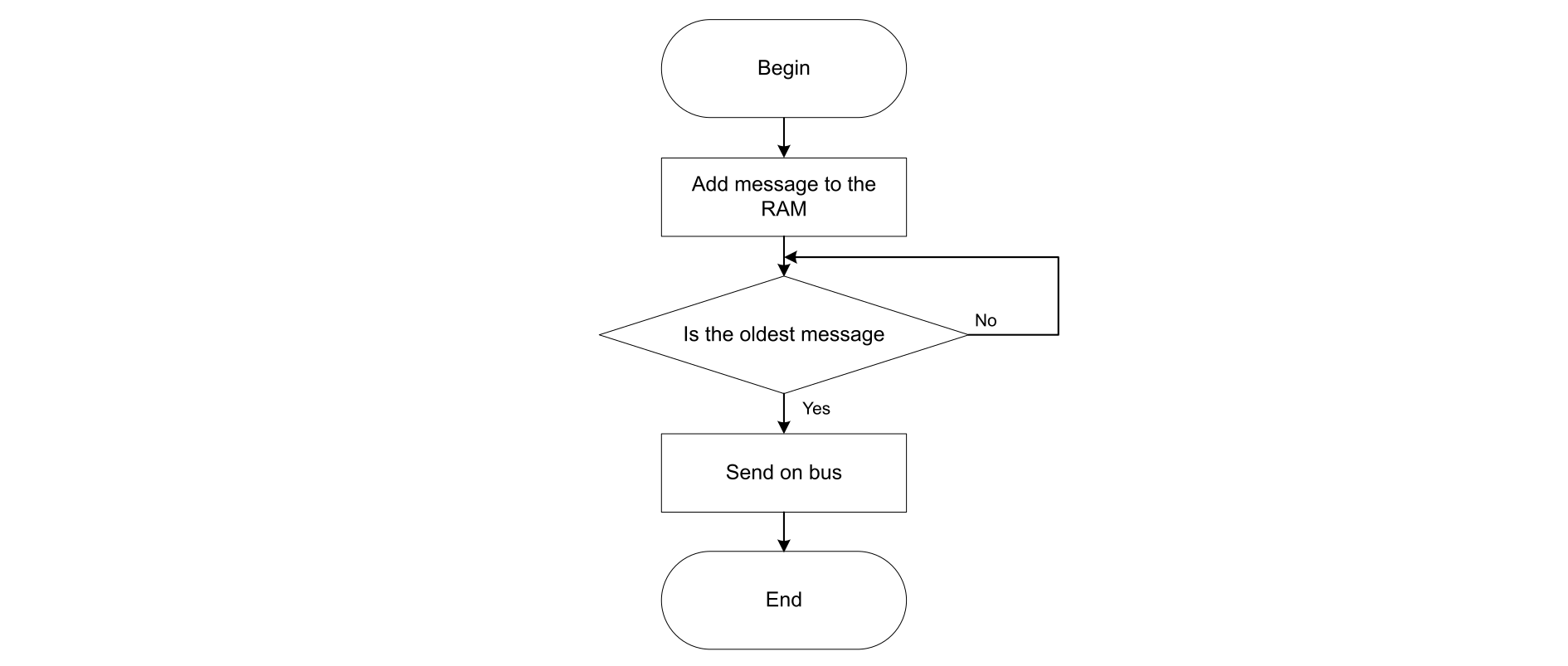
The following flow chart shows a simplified operation of the transmission with Tx FIFO mechanism.
Figure 16. Transmission with Tx FIFO mechanism
Tx queue
Tx queue operation is configured by writing 1 to the TFQM bit in FDCAN_TXBC. The elements stored in the Tx queue are transmitted starting with the Tx queue buffer with the lowest Identifier (highest priority).
In contrast to dedicated Tx buffers, the position on the RAM is automatically and dynamically managed so the message identifier is not fixed to a predefined Tx buffer index.
New messages have to be written to the Tx queue buffer referenced by the put index. An add request cyclically increments the put index to the next free Tx queue buffer. The fact that Tx queue is full is indicated by the TFQF bit set to 1 in FDCAN_TXFQS. No further element must be written to the Tx queue until at least one of the requested elements is sent out or a pending transmission request is cancelled.
The memory requirements for the Tx queue buffer depend on the number of data bytes belonging to Tx queue element.
The address of a next available free Tx queue buffer in the CAN message RAM can be calculated by the following formula:
Next free Tx queue buffer address = CAN_message_RAM_base_address + FDCAN_TXBC.TBSA (start address) + FDCAN_TXFQS.TFQPI (put index) x Tx_Buffer_element_size
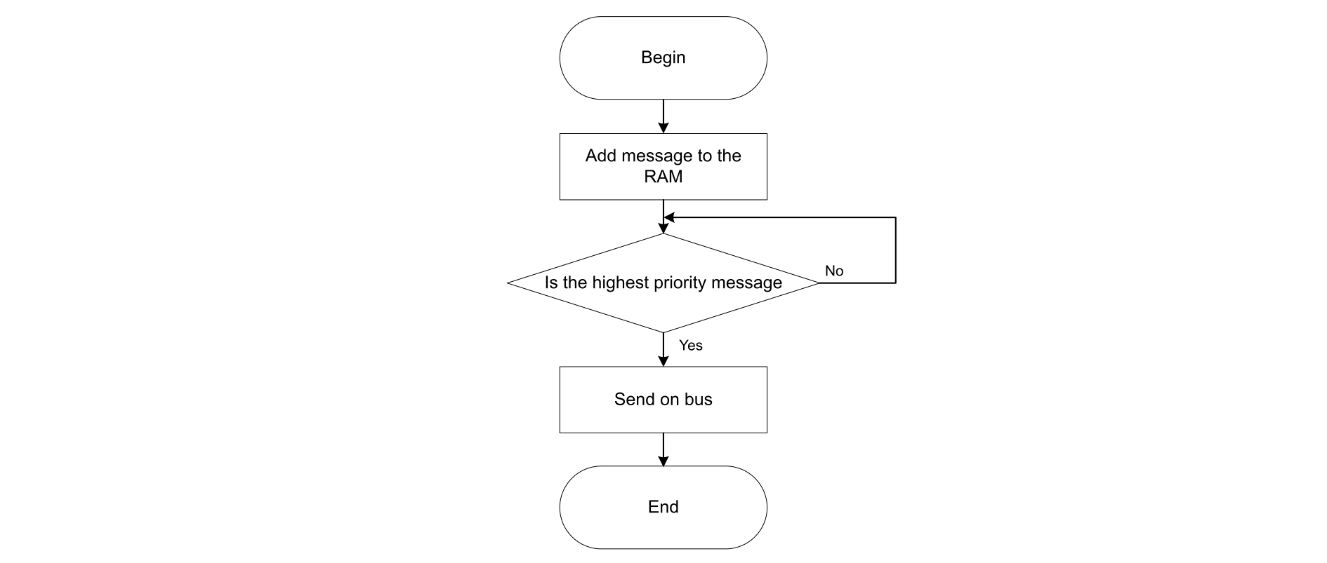
The following flow chart shows a simplified operation of the transmission with Tx queue mechanism.
Figure 17. Transmission with Tx queue mechanism
Differences between dedicated Tx buffer, Tx FIFO and Tx queue
The differences between a dedicated Tx buffer, a Tx FIFO and a Tx queue are described in the table below.
Table 7. Differences between dedicated Tx buffer, Tx FIFO and Tx queue
Feature
Dedicated Tx buffer
Tx FIFO
Tx queue
Sections that can be configured
32 dedicated Tx buffers can be configured.
One Tx FIFO can configured.
One Tx queue can configured.
Elements per section
Tx buffer is configured to contain only one element per buffer.
May contain one or more elements per section (up to 32)
May contain one or more elements per section (up to 32)
Element to be sent first
Element with the lowest ID is sent first.
Elements transmitted in the FIFO order
Element with the lowest ID is sent first.
Behaviour if multiple elements with the same ID are present
The first transmission request is sent first.
No prioritization with identifier
FIFO order
Position in the RAM
User chooses the buffer index.
Automatically and dynamically managed (using the incrementing of get and put index)
Pending elements management
Elements become pending after being added to the RAM or after the tx buffer request is enabled.
Elements become pending after being added to the RAM (the request is automatically enabled).
Flexible transmission configuration
An efficient FDCAN supports mixed configurations to allow more flexibility on transmissions and to take the best advantage of each mechanism benefits. The supported mixed configurations are dedicated Tx buffer + Tx FIFO and dedicated Tx buffer + Tx queue.
Mixed configuration: dedicated Tx buffers and Tx FIFO
The Tx buffer section of the CAN message RAM can be configured with a mixed configuration, where the Tx buffers section in the CAN message RAM is subdivided into a set of dedicated Tx buffers and a Tx FIFO.
The number of dedicated Tx buffers is configured via NDTB[5:0] in FDCAN_TXBC. The number of Tx buffers assigned to the Tx FIFO is configured via TFQS[5:0] in FDCAN_TXBC.
The Tx handler scans all the dedicated Tx buffers with an activated transmission request and the oldest pending Tx FIFO buffer referenced by the get index. The buffer with the lowest identifier gets the highest priority and is transmitted next.
A use case using a mixed dedicated Tx buffer and a Tx FIFO is illustrated in the figure below.
Figure 18. Mixed configuration with dedicated Tx buffers and Tx FIFO
In this example, the elements are transmitted in the following order (assuming that all dedicated Tx buffers requests are enabled):
Tx buffer 3 (identifier = 1: it is the highest priority between all other dedicated Tx buffers and it has a higher priority than the oldest pending Tx FIFO: Tx buffer 7)
Tx buffer 0 (identifier = 3: it is the highest priority between all other dedicated Tx buffers and it has higher priority than the oldest pending Tx FIFO: Tx buffer 7)
Tx buffer 7 (because it is the oldest pending Tx FIFO with identifier =4 and has higher priority between all dedicated Tx buffers)
Tx buffer 8 (because it is the oldest pending Tx FIFO with identifier =2 and has the highest priority between all dedicated Tx buffers)
Tx buffer 4 (identifier = 8: it has the highest priority between all other dedicated Tx buffers and the Tx FIFO is empty)
Tx buffer 2 (identifier = 12: it has the highest priority between all other dedicated Tx buffers and the Tx FIFO is empty)
Tx buffer 1 (identifier = 15: it has the highest priority between all other dedicated Tx buffers and the Tx FIFO is empty)
Tx buffer 5 (because it is the only pending dedicated Tx buffer)
Mixed configuration: dedicated Tx buffers and Tx queue
The Tx buffer section of the CAN message RAM can be configured with a mixed configuration where the Tx buffers section in the CAN message RAM is subdivided into a set of dedicated Tx buffers and a Tx queue.
The number of dedicated Tx buffers is configured via NDTB[5:0] in FDCAN_TXBC and the number of Tx queue buffers is configured via TFQS[5:0] in FDCAN_TXBC.
The Tx handler scans all the dedicated Tx buffers with activated transmission request and the Tx queue buffers. The buffer with the lowest identifier gets the highest priority and is transmitted next.
A use case using a mixed dedicated Tx buffer and a Tx queue is illustrated in the figure below.
Figure 19. Mixed configuration with dedicated Tx buffers and Tx queue
In this example, the messages are transmitted in the following order (assuming that all dedicated Tx buffers request are enabled):
Tx buffer 3 (identifier = 1: it is the highest priority between all other Tx buffers)
Tx buffer 8 (identifier = 2: it is the highest priority between all other Tx buffers)
Tx buffer 0 (identifier = 3: it is the highest priority between all other Tx buffers)
Tx buffer 7 (identifier = 4: it is the highest priority between all other Tx buffers)
Tx buffer 4 (identifier = 8: it is the highest priority between all other Tx buffers)
Tx buffer 2 (identifier = 12: it is the highest priority between all other Tx buffers)
Tx buffer 1 (identifier = 15: it is the highest priority between all other Tx buffers)
Tx buffer 5 (because it is the only pending Tx buffer)
Note:
The mixed configuration with Tx FIFO and Tx queue is not supported.
Differences between mixed configuration of dedicated buffer + Tx FIFO and mixed configuration of Tx buffer + Tx queue
The main differences between the mixed configurations Tx buffer + Tx queue and Tx buffer + Tx FIFO are presented in the table below.
Table 8. Differences between mixed Tx buffer + Tx FIFO and mixed Tx buffer + Tx queue configurations
Feature
Mixed configuration: Tx buffer + Tx queue
Mixed configuration: Tx buffer + Tx FIFO
Description
A combination of dedicated Tx buffers and Tx queue
A combination of dedicated Tx buffers and Tx FIFO
Element to be sent first
Element with the lowest ID between all dedicated Tx buffers and Tx queue
Element with the lowest ID between all dedicated Tx buffers and oldest element in Tx
Management of multiple elements with same ID
First request is sent first.
Order request FIFO
Note:
In Tx FIFO + Tx queue, elements become pending just after the “add to the RAM” action.
Test modes
Within the operation mode of a FDCAN, several test modes are available besides the normal operation. There test modes must be used for production tests or self-test only and for the calibration unit.
The TEST bit in FDCAN_CCCR must be set to 1 to enable a write access to the FDCAN test register and the configuration of test modes and functions.
The FDCAN works in one of the following modes:
Restricted-operation mode
Bus-monitoring mode
External loop-back mode
Internal loop-back mode
Restricted-operation mode
In restricted-operation mode, the FDCAN is able:
to receive data frames
to receive remote frames
to give acknowledge to valid frames
This mode does not support:
data frames sending
remote frames sending
active error frames or overload frames sending
The FDCAN is set in the restricted-operation mode via the ASM bit in FDCAN_CCCR.
The restricted-operation mode is automatically entered when the Tx handler is not able to read data from the CAN message RAM on time or when the clock calibration is active.
In this mode, the application tests different bit rates and leaves the restricted-operation mode after the application received a valid frame.
The following figure illustrates the connection of FDCAN_TX and FDCAN_RX pins in restricted-operation mode.
Figure 20. Pin control in restricted-operation mode
Note:
FDCAN_TX pin is recessive as long as FDCAN is in restricted-operation mode. A dominant bit is transmitted to acknowledge the reception of a valid frame.
Bus-monitoring mode
In order to analyze the traffic on the bus without affecting it by the transmission of dominant bits, the user can set the FDCAN in bus‑monitoring mode via the MON bit in FDCAN_CCCR.
In bus-monitoring mode, the FDCAN is able:
to receive valid data frames
to receive valid remote frames
This mode does not support:
transmission start
acknowledge to valid frames (difference versus the restricted-operation mode)
In the bus-monitoring mode, the FDCAN only sends recessive bits on the bus. The figure below shows the connection of FDCAN_TX and FDCAN_RX pins in bus-monitoring mode.
Figure 21. Pin control in bus-monitoring mode
External loop-back mode
This mode is provided for hardware self-test. The user can set the FDCAN in external loop-back mode by writing 1 to the LBCK bit in FDCAN_TEST and by writing 0 to the MON bit in FDCAN_CCCR. The FDCAN treats its own transmitted messages as received messages and stores them if they pass the acceptance filtering in Rx FIFO.
In order to be independent from the external stimulation, the FDCAN ignores acknowledge errors (recessive bit sampled in the acknowledge slot). The FDCAN performs an internal feedback from its “transmit” output to its “receive” input.
The following figure shows the connection of FDCAN_TX and FDCAN_RX pins in external loop‑back mode.
Figure 22. Pin control in external loop-back mode
Internal loop-back mode
This mode is provided for hardware self-test. The user can set the FDCAN in internal loop-back mode via by writing 1 to the LBCK bit in FDCAN_TEST and by writing 1 to the MON bit in FDCAN_CCCR.
The FDCAN can be tested without affecting a running CAN system connected to the FDCAN_TX and FDCAN_RX pins. FDCAN_RX pin is disconnected from the FDCAN and FDCAN_TX pin is held recessive.
The figure below shows the connection of FDCAN_TX and FDCAN_RX pin in internal loop-back mode.Figure 23. Pin control in internal loop-back mode
Transceiver delay compensation
At the sample point, all transmitters check whether the previously transmitted bit is sampled correctly. This mechanism is needed to check for problems and to detect other node error frames. Since the transmitter sees its own transmitted bits delayed by the transceiver loop delay, this delay sets a lower limit to the TSEG1 as shown in the figure below (time segment before sample point), that is also an upper limit to the data bit rate. This is the reason why the transceiver delay compensation mechanism (TDC) was introduced.
Figure 24. Bit timing
In order to compensate this loop delay when checking for bit errors, a secondary sample-point (SSP) is defined. Instead of being done at the sample point, the transmitted bits are checked at the SSP. The result of that check is stored until the next sample point is reached.
An SSP is generated for each bit transmitted in the data phase. Transceiver asymmetry and ringing on the bus have to be considered for the SSP position, but there is no clock tolerance, since the transceiver monitors its own bit stream.
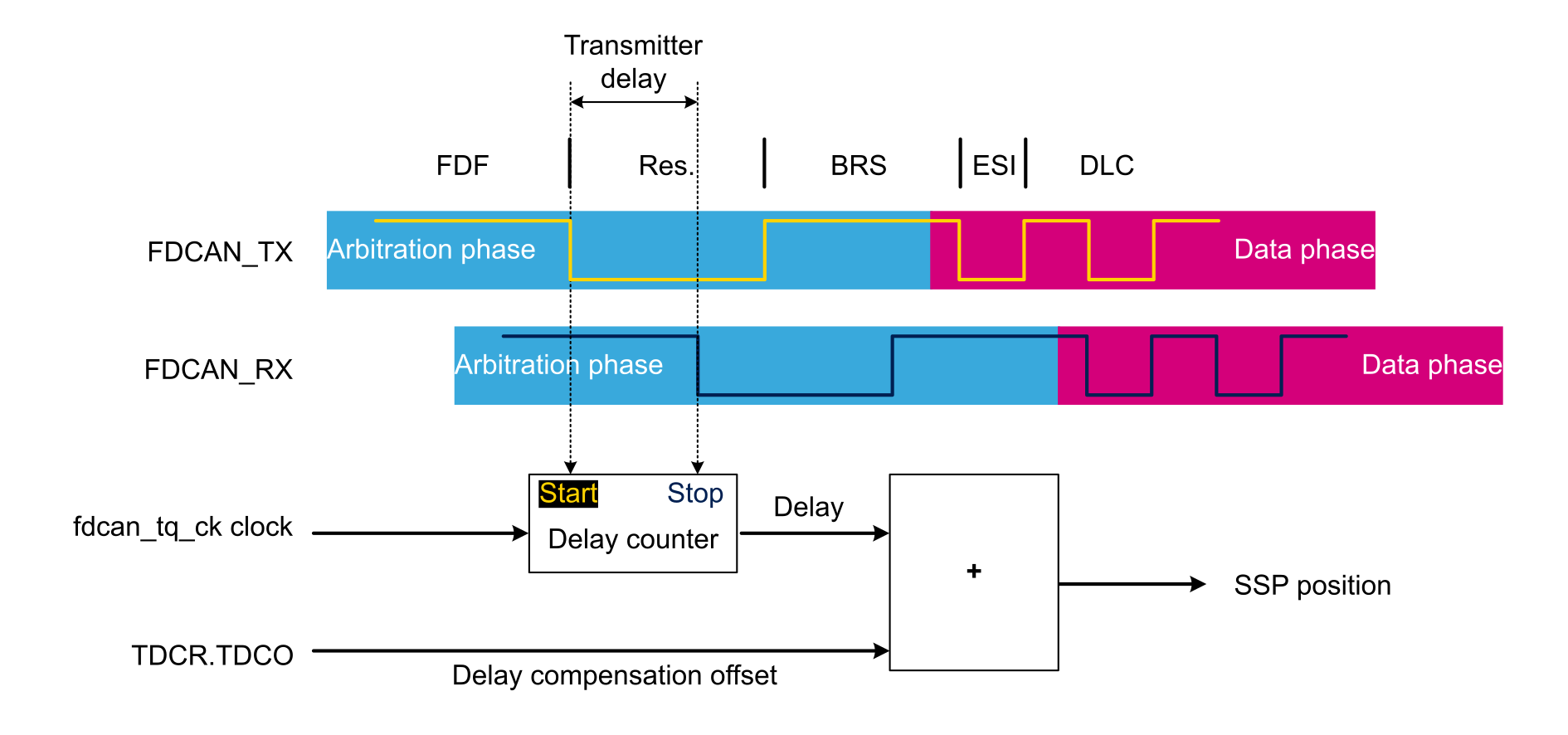
The transceiver delay compensation is enabled by writing 1 to the TDC bit in FDCAN_DBTP. The measurement starts within each transmitted FDCAN frame before the beginning of the data phase (at the falling edge of the FDF bit to bit res). The measurement stops when this edge is seen at the “receive” input pin FDCAN_RX of the transmitter. The resolution of this measurement is 1 mtq (minimum time quantum).
The following figure presents the measurement of loop delay.
Figure 25. Loop delay measurement
Note:
During the arbitration phase, the delay compensation is always disabled.
The SSP position is defined as the sum of the measured delays from the FDCAN_TX pin to the FDCAN_RX pin, plus the transmitter delay compensation offset as configured via the TDCO[6:0] field in FDCAN_TDCR.
Note:
The transmitter delay compensation offset is used to adjust the position of the SSP inside the received bit.
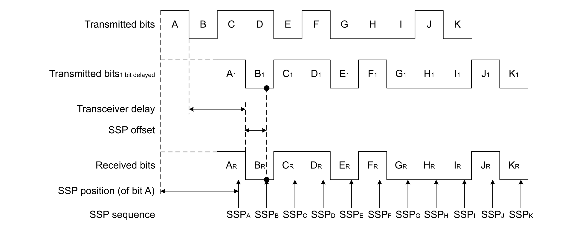
The value of a transmitted bit is stored until its SSP is reached, then it is compared with the actually received bit value, as in figure below, that shows a transmitted bit sequence A to K and a received bit sequence AR to KR, together with a sequence of SSPs from SSPA to SSPK. The received bit BR is checked at SSPB by comparing it with the delayed bit B1. The position of SSPB is at a specific time after the start of the transmitted bit B. This specific time is the sum of the measured transceiver delay and the configured SSP offset.
Figure 26. SSP position in transmit delay-compensation
As determined in Bosch documentation, the following boundary conditions have to be considered for the transmitter delay compensation implemented in the FDCAN:
The sum of the measured delay from FDCAN_Tx to FDCAN_Rx and the configured transmitter delay compensation offset mus t be less than six bit times in the data phase.
The sum of the measured delay from FDCAN_Tx to FDCAN_Rx and the configured transmitter delay compensation offset mus t be less or equal 127 mtq.
Note:
If the sum exceeds 127 mtq, the maximum value (127 mtq) is used for transmitter delay compensation.
The data phase ends at the sample point of the CRC delimiter that stops checking received bits at the SSPs.
The next part of this document explains the clock calibration unit with a description of its utility and operation.
Clock calibration on FDCAN
The FDCAN supports the clock calibration unit (CCU) feature. This feature allows a user to calibrate a FDCAN receiver (device) by a FDCAN transmitter (host). For example, when the FDCAN device communicates with the newest bitrate of the host.
This feature allows the user to add a new instance in the bus and the existence of the bitrate is unknown. It is also useful when the FDCAN receiver does not have a precise quartz (can cause an error on time).
CCU description
The clock calibration unit is initialized via the FDCAN_CCU_CCFG register, that can be written only when both CCE and INIT bits are set to 1 in FDCAN_CCCR.
The CCU is only possible when the FDCAN operates in CAN 2.0 mode.
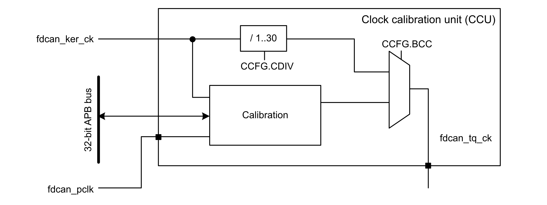
The clock calibration is bypassed when BCC = 1 in FDCAN_CCU_CCFG. The following figure shows the bypass operation.
Figure 27. Bypass operation of the CCU
CCU operating conditions
The CCU operates only when the FDCAN bitrate is between 125 Kbit/s and 1 Mbit/s.
CCU functional description
The calibration of fdcan_tq_ck (time quanta clock) via CAN messages is performed by adapting a clock divider that generates the CAN protocol time quantum, tq, from the fdcan_ker_ck clock.
Calibration of the state machine
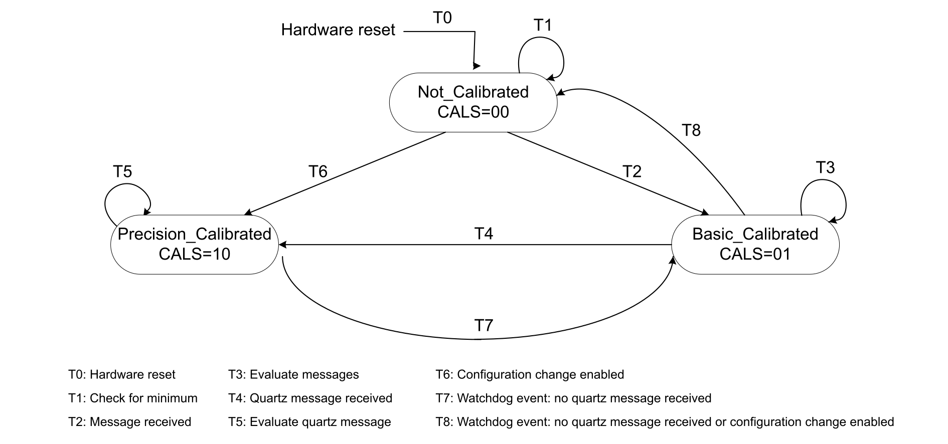
The calibration of the functional state machine is illustrated below.
Figure 28. Functional state machine calibration
Basic calibration
The minimum distance between two consecutive falling edges from recessive to dominant is measured. This measure assumes two CAN bit times counted in PLL clock periods. The clock divider is updated each time a new measurement finds a smaller distance between edges by the CDIV[3:0] field in FDCAN_CCU_CCFG. A basic calibration is achieved when the CAN protocol controller detects a valid CAN message.
Precision calibration
The calibration state machine measures the length of a longer bit sequence inside a CAN frame by counting the number of fdcan_ker_ck periods. The length of this bit sequence can be configured to 32 or 64 bits by the CFL bit in FDCAN_CCU_CCFG. Precision calibration is based on the new clock divider value, calculated from the measurement of the longer bit sequence.
Calibration frames are detected by the FDCAN acceptance filtering. A filter element and an Rx buffer must be configured in the FDCAN to identify and store the calibration messages.
If the fdcan_ker_clk calibration is done by software (evaluating the calibration status from CALS[1:0] field in FDCAN_CCU_CSTAT), the FDCAN must be set in restricted-operation mode until the calibration is in Precision_Calibrated state (no frame and no error or overload flag transmission, no error counting).
Note:
After reception of a calibration message, the Rx buffer new data flag must be reset to enable signaling of the next calibration message.
The data field of the calibration message must be at least 1010 binary sequence to ensure that the device node can enter the Basic_Calibrated state, and that the host node messages are acknowledged.
Precision calibration can be performed only on valid CAN frames transmitted by a host node with a stable quartz-controlled clock. Precision calibration must be repeated in predefined maximum intervals supervised by the calibration watchdog.
Calibration watchdog
The calibration watchdog is a down counter, that starts in not Not_Calibrated state and that monitors the received messages.
When in Basic_Calibrated state, the calibration watchdog is restarted with each received message.
Note:
In case no message is received until the calibration watchdog counted down to zero, the FSM calibration stays in Not_Calibrated state. The counter is reloaded and basic calibration restarts.
When Precision_Calibrated state is entered, the calibration watchdog is restarted. In this state, the calibration watchdog monitors the quartz message received.
Note:
In case no message from a quartz-controlled node is received by the FDCAN until the calibration watchdog counted down to zero, the FSM calibration transits back to “Basic_Calibrated” state.
Calibration example
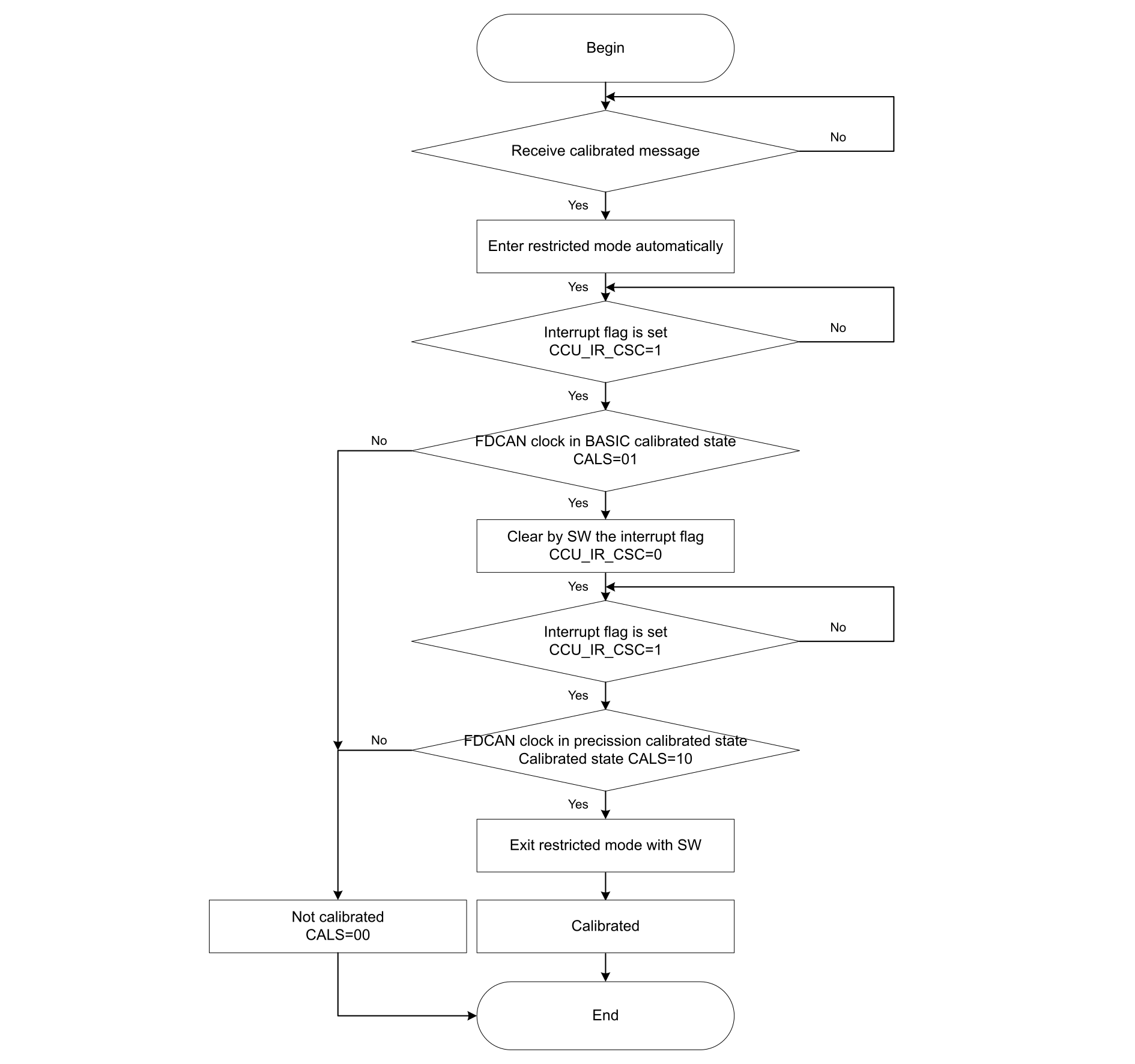
This example presents a use case to calibrate an FDCAN device (receiver) by an FDCAN host (transmitter). The following flow chart illustrates the steps through the FDCAN device before calibrating.
Figure 29. Steps to calibrate a FDCAN device
After the calibration passed successfully, the FDCAN device becomes ready for reception and transmission messages with the new FDCAN host bitrate.