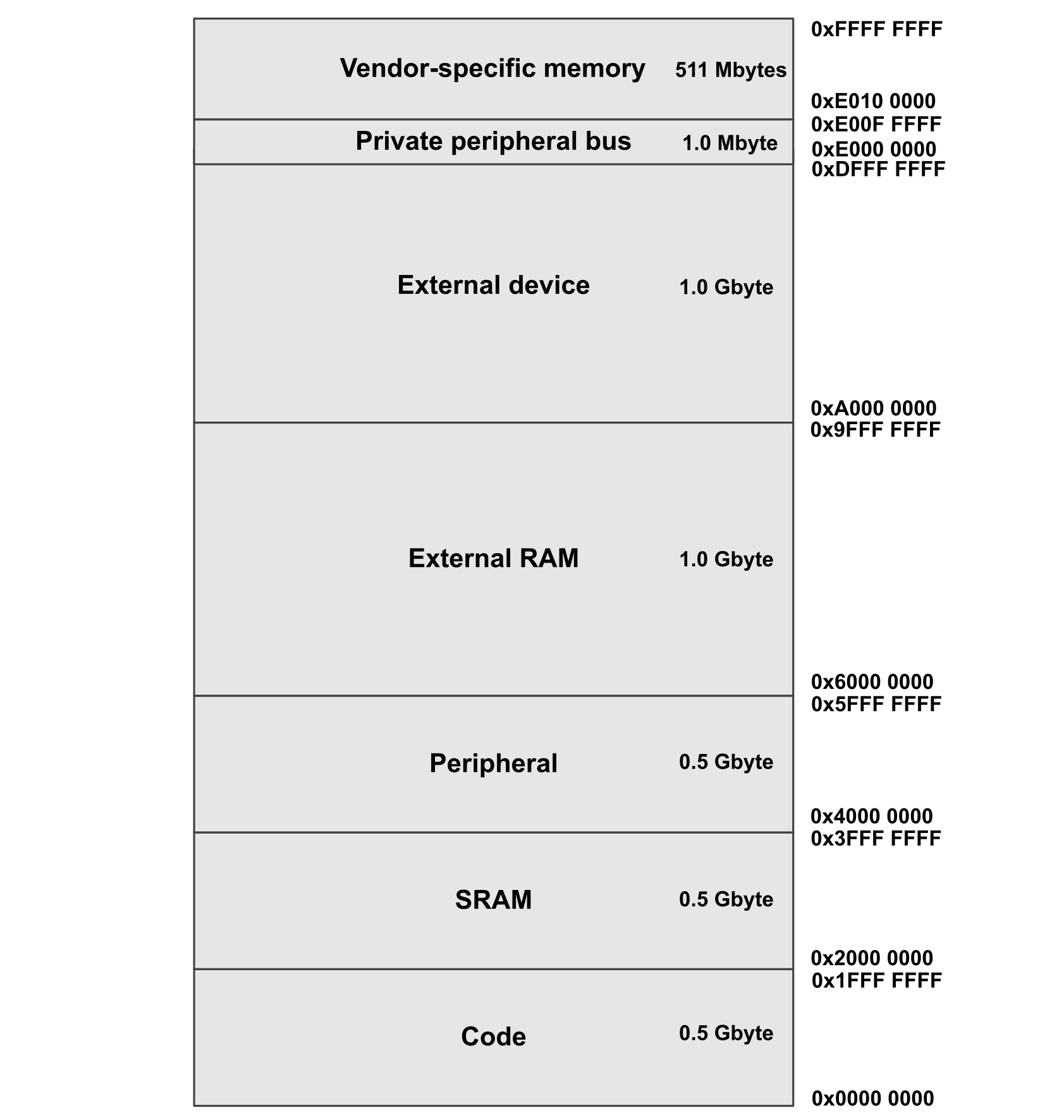
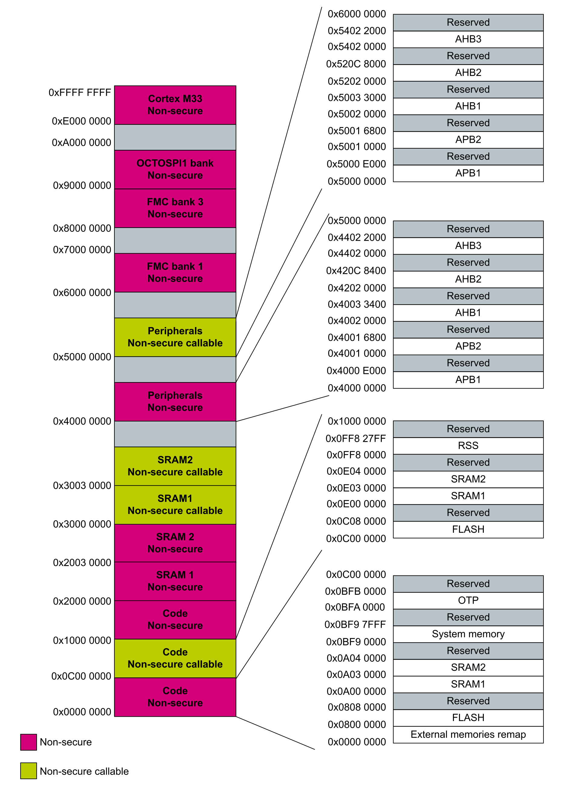
Overview
The MPU can be used to make an embedded system more robust and more secure by:
- prohibiting the user applications from corrupting data used by critical tasks (such as the operating system kernel)
- defining the SRAM memory region as a non-executable (execute never XN) to prevent code injection attacks
- changing the memory access attributes
The MPU can be used to protect up to 16 memory regions. In Armv6 and Armv7 architecture (Cortex-M0+, M3, M4, and M7, these regions in turn can have eight subregions, if the region is at least 256 bytes. The exact amount of regions protected can vary between core and devices in the STM32, refer to Table 6 MPU register summary for more details. The subregions are always of equal size, and can be enabled or disabled by a subregion number. Because the minimum region size is driven by the cache line length (32 bytes), eight subregions of 32 bytes correspond to a 256-byte size.
The regions are numbered 0 to 15. In addition, there is a region called the default region with an id of -1. All the 0-15 memory regions take priority over the default region.
The regions can overlap, and can be nested. The region 15 has the highest priority and the region 0 has the lowest one and this governs how overlapping the regions behave. The priorities are fixed, and cannot be changed.
In Armv8 architecture (Cortex-M33 and M55) the regions are defined using a base and a limit address offering flexibility and simplicity to the developer on the way to organize them. Additionally, Cortex-M33 and M55 do not include subregions as the region size is now more flexible.
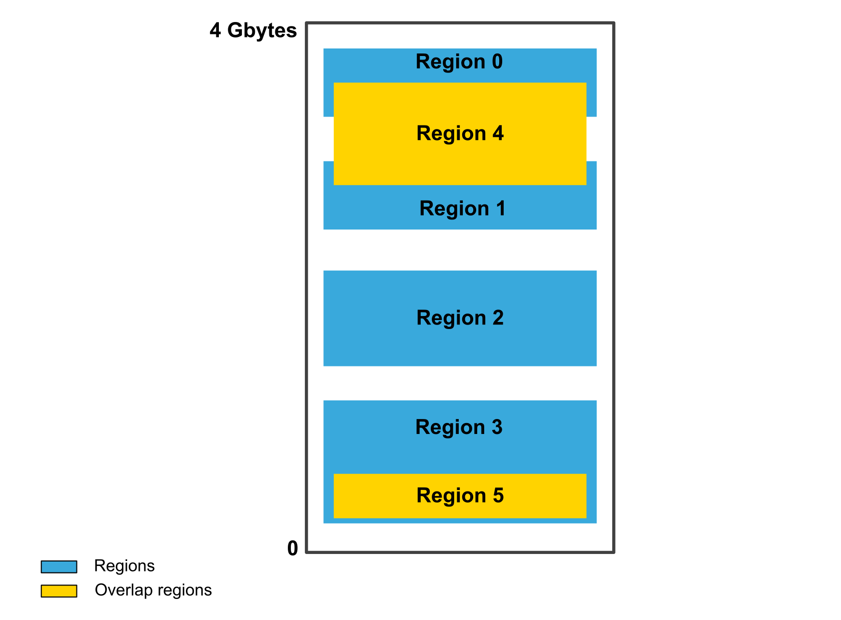
In Armv8 architecture, regions are now not allowed to overlap. As the MPU region definition is much more flexible, overlapping MPU regions is not necessary.
The MPU is unified, meaning that there are not separate regions for the data and the instructions.
The MPU can be used also to define other memory attributes such as the cacheability, which can be exported to the system level cache unit, or to the memory controllers. The memory attribute settings in Arm® architecture can support two levels of cache: inner cache and outer cache. For the STM32F7 and STM32H7 series, only one level of cache (L1-cache) is supported.
The cache control is done globally by the cache control register, but the MPU can specify the cache policy and whether the region is cacheable or not.