AN4838 · Application noteIntroduction to memory protection unit management on STM32 MCUs
Download .pdfOpen in the full document

Cortex-M7 constraint speculative prefetch

Cortex-M7 constraint speculative prefetch

The Cortex-M7 implements the speculative prefetch feature, which allows speculative accesses to normal memory locations (for example: FMC, Quad-SPI devices). When a speculative prefetch happens, it may impact memories or devices that are sensitive to multiple accesses (such as FIFOs, LCD controller). It may also disturb the traffic generated by another masters such as LCD-TFT or DMA2D with higher bandwidth consumption when a speculative prefetch happens. In order to protect normal memories from a speculative prefetch, it is recommended to change memory attributes from normal to a strongly ordered or to device memory thanks to the MPU. For more details about configuring memory attributes, refer to MPU setting example with STM32Cube HAL on Armv6 and Armv7 architectures.
Cortex-M33/M55 memory types, registers and attributes

Cortex-M33 and Cortex-M55 are respectively based on the Armv8-M and Armv8.1-M architectures (Cortex®-M55 processor supports Arm Protected Memory System Architecture (PMSA)). In both cases, the MPU is a component that is primarily used for memory region protection.

Although the concepts for the MPU operations are similar, the MPU in the Armv8-M architecture has a different programmers’ model to the MPU in previous versions of the M-profile Arm® architecture.

It is important to realize that all MPU registers are banked. If Arm TrustZone® is enabled, there is a set of MPU registers for the secure state, and a mirror set for the non-secure state. When accessing the MPU address between 0xE000 ED90 and 0xE000 EDC4, the type of MPU registers accessed is determined by the current state of the processor.

Non-secure code can access non-secure MPU registers and secure code can access secure MPU registers. Secure code can access non-secure MPU registers at their aliased address.

Secure access sees secure MPU registers, non-secure access sees non-secure MPU registers. Secure software can also access non-secure MPU registers using the alias address.

Note:

See Arm®-M Architecture reference manual for more information about the memory model.

Memory types and attributes

In Armv8-M and Armv8.1-M architectures, memory types are divided into:
  • normal memory
  • device memory
Note:

The strongly ordered (SO) device memory type in Armv6-M and Armv7-M is now a subset of the device memory type.

A normal memory type is intended to be used for MPU regions that are used to access general instruction or data memory. Normal memory allows the processor to perform some memory access optimizations, such as access reordering or merging. Normal memory also allows memory to be cached and is suitable for holding executable code. Normal memory must not be used to access peripheral MMIO registers. The device memory type is intended for that use. A normal memory definition remains mostly unchanged from the Armv7-M architecture.

A normal memory has the following attributes:
  • cacheability: memories cacheable or non-cacheable
  • shareability: normal memory shareable or non-shareable
  • execute never: memories marked as executable or execute never (XN)

A device memory must be used for memory regions that cover peripheral control registers. Some of the optimizations that are allowed to normal memory, such as access merging or repeating, are unsafe to a peripheral register.

A device memory has the following attributes:
  • G or nG: gathering or non-gathering. (multiple accesses to a device can be merged into a single transaction except for operations with memory ordering semantics, for example, memory barrier instructions, load acquire/store release).
  • R or nR: reordering
  • E or nE: early write acknowledge (similar to bufferable)
Only four combinations of these attributes are valid:
  • device-nGnRnE: equivalent to Armv7-M strongly ordered memory type
  • device-nGnRE: equivalent to Armv7-M device memory
  • device-nGRE: new to Armv8-M
  • device-GRE: new to Armv8-M

Cortex-M55 access privilege level for device and normal memory

The AMBA® 5 AXI, AMBA® 5 AHB, and AMBA® 4 APB protocols have signals that can report the privilege level of an access request to the system.

The Cortex-M55 processor supports these signals across the manager AXI (M-AXI), the peripheral AHB (P-AHB), and the external private peripheral bus (EPPB) interfaces for device memory. It also supports privilege reporting for normal memory on P-AHB. However, accesses to normal memory on M-AXI can be buffered and cached, allowing memory read and write requests, as well as instruction fetches from both privileged and unprivileged software, to be merged. For these transactions initiated by loads and stores, the AXI signals ARPROT[0] and AWPROT[0] are always 1 indicating a privileged access. Access permission to a region of memory can always be restricted to software running in privileged mode by using the MPU.

The instruction tightly coupled memory (ITCM) and data tightly coupled memory (DTCM) interfaces provide the following signals: ITCMPRIV, D0TCMPRIV, D1TCMPRIV, D2TCMPRIV, and D3TCMPRIV. These signals indicate the privilege of all memory accesses except the ones initiated by loads and stores.

Attribute indirection

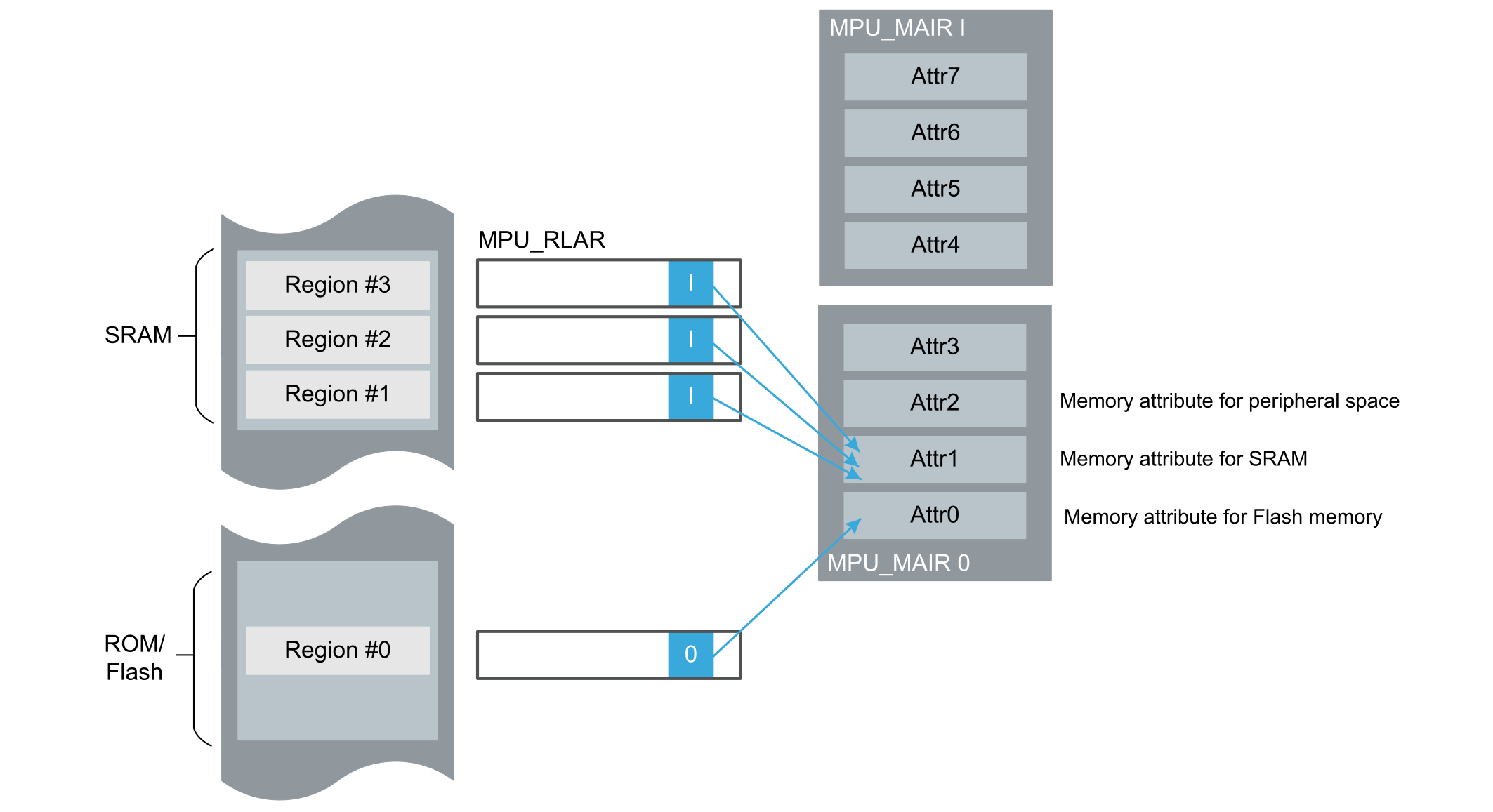
The attribute indirection mechanism allows multiple MPU regions to share a set of memory attributes.

The MPU can be configured to support 0, 4, 8, 12, or 16 memory regions (security extension is included in the Cortex‑M55 processor. Memory protection can be duplicated between secure and nonsecure MPU (MPU_S and MPU_NS).)

The number of regions in the secure and nonsecure MPU can be configured independently, and each can be programmed to protect memory for the associated security state.

The following figure shows that MPU regions 1, 2, and 3 are all assigned to SRAM. Therefore, they can share cache-related memory attributes.

Figure 4. Attribute indirection example

At the same time, regions 1, 2, and 3 can still have their own access permission, XN, and shareability attributes. This is required as each region can be used differently in the application.

MPU registers

The Cortex-M33/M55 MPU registers are different from previous Cortex® cores, offering more flexibility and compatibility with Arm® TrustZone®. Consequently, the programming approach used in previous products cannot be applied for these ones. The introduction of the MPU Region Base Limit Register, for example, allows the user to easily define start and end of their protected regions.
Table 6. MPU register summary
AdressNameTypeReset valueDescription
0xE000ED90MPU_TYPE1RO0x0000xx00
0xE000ED94MPU_CTRLRW0x00000000

MPU Type Register

0xE000ED98MPU_RNRRW0x000000XX

MPU Control Register

0xE000ED9CMPU_RBARRWUnknown

MPU Region Number Register

0xE000EDA0MPU_RLARRWUnknown, bit [0] resets to 0

MPU Region Base Address Register

0xE000EDA4MPU_RBAR_A1RWUnknown

MPU Region Limit Address Register

0xE000EDA8MPU_RLAR_A1RWUnknown

MPU Region Base Address Register Alias 1

0xE000EDACMPU_RBAR_A2RWUnknown

MPU Region Limit Address Register Alias 1

0xE000EDB0MPU_RLAR_A2RWUnknown

MPU Region Base Address Register Alias 2

0xE000EDB4MPU_RBAR_A3RWUnknown

MPU Region Limit Address Register Alias 2

0xE000EDB8MPU_RLAR_A3RWUnknown

Address Register Alias 3

0xE000EDC0MPU_MAIR0RWUnknown.

MPU Memory Attribute Indirection Register 0

0xE000EDC4MPU_MAIR1RWUnknown

MPU Memory Attribute Indirection Register 1

1 MPU_TYPE[15:8] depends on the number of MPU regions configured. This value can be 0, 4, 8, 12, or 16.

MPU features comparison between Cortex cores

There are few MPU differences between Cortex-M0+, Cortex-M3/M4, Cortex-M7, Cortex‑M33 and Cortex‑M55.The user must be aware of them if the MPU configuration software has to be used. The table below illustrates these differences.
Table 7. Comparison of MPU features between Cortex cores
FeaturesCortex-M0+Cortex-M3/M4Cortex-M7Cortex-M33Cortex-M55
Number of regions888/16 128 MPU_S / 8 MPU_NS316 MPU_S / 16 MPU_NS
Region addressYesYesYesYesYes
Region size256 bytes to 4 Gbytes32 bytes to 4 Gbytes32 bytes to 4 Gbytes32 bytes to 4 Gbytes32 bytes to 4 Gbytes
Region memory attributesS, C, B, XN4TEX, S, C, B, XNTEX, S, C, B, XNS,C, E 5,G 6, R 7, XNS,C, E5 ,G 6, R 7, XN, PXN8
Region access permission (AP)YesYesYesYes (privileged or not)Yes (privileged or not)
Subregion disable8 bits8 bits8 bitsNANA
MPU bypass for NMI/HardFaultYesYesYesYesYes
Alias of MPU registersNoYesYesYesYes
Fault exceptionHardFault onlyHardFault/MemManageHardFault/MemManageHardFault/MemManageHardFault/MemManage
1 For STM32H7 series devices.
2 For STM32F7 series devices.
3 For STM32H5/STM32U3: 12 MPU_S / 8 MPU_NS .
4 Cortex-M0+ supports one level of cache policy. That is why the TEX field is not available in Cortex-M0+ processor.
5 Early write acknowledge (similar to bufferable)
6 Gathering
7 Reordering
8 Privileged eXecute Never attribute in Armv8.1-M architecture.