AN4879 · Application noteIntroduction to USB hardware and PCB guidelines using STM32 MCUs
Download .pdfOpen in the full document

VBUS sensing detection

VBUS sensing detection

Based on the USB specification, a USB device must use VBUS sensing detection. When the device detects the host presence, it connects its pull-up resistor to either a D+ or D- data signal. This allows the host to detect the device presence on the bus.

There are two cases:
  • The USB device is bus-powered. VBUS sensing is not mandatory (USB is always connected when the device is powered)
  • The device is self-powered. VBUS sensing is mandatory.

Pin PA9, a five volt-tolerant pin, which includes an additional function natively dedicated to VBUS sensing. The absolute maximum ratings table of the datasheet indicates that the five volt-tolerant pin voltage cannot exceed VDD + 4 V. The user must avoid the situation when the MCU is not powered, and a 5 V VBUS is connected to PA9: this violates the condition on absolute maximum ratings, and can result in permanent damage to the device. For this purpose, it is mandatory to reduce the voltage on PA9 below 4 V.

For a reliable and safe VBUS detection, the use of a voltage divider is recommended to guarantee absolute maximum ratings.
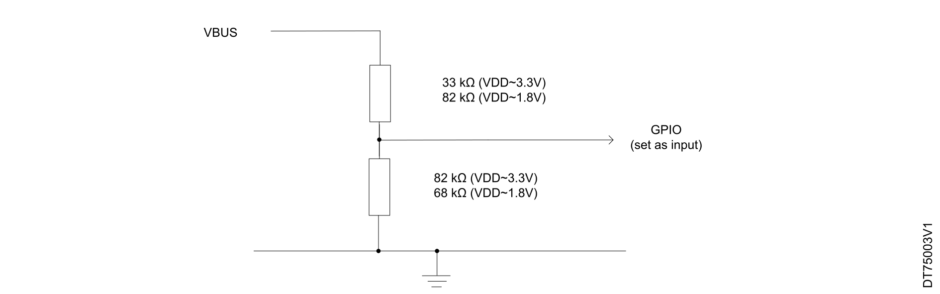
Simple resistor divider

To minimize the DC current, the total resistance between VBUS and GND must be high. The basic GPIO input levels (VIL, VIH) can now be used with the resistor divider. As this method uses the regular GPIO functionality, the VBUS sensing function (OTG_GCCFG.VBDEN), embedded in PA9, should not be enabled.

The GPIOs available in STM32 families exhibit varying maximum operating conditions at their inputs. These conditions are typically restricted to a value that depends on certain VDDs. For instance, the expression min(VDD, VDDA, VDD3V3_USB, VBAT) +3.9 represents one such example. To detect VBUS through GPIOs, it is imperative to adhere to these tolerances even in the absence of VDDs. In the worst-case scenario (that is, absence of all VDDs), the aforementioned expression would yield a value of 3.9 V. This higher tolerance enables easier detection. However, if the guaranteed input tolerance is less than 3.6 V, a different approach is required.

Note:

For the VIL/VIH calculation, all GPIOs are powered by the main I/O supply VDD. The VDDUSB is dedicated in some MCUs to the USB signals.

The recommended resistor divider values for VBUS detection are the following:
  • For VDD in the 3.0-3.6 V range: 82 kΩ (to GND), 33 kΩ (to VBUS).
  • For VDD in the 1.65-2.0 V range: 68 kΩ (to GND), 82 kΩ (to VBUS).

Resistor values have been assessed assuming a ± 1% tolerance. They are checked against VIL/VIH across the different STM32 families, to guarantee switching when VBUS is between 0.8 and 3.67 V.

Note:

This solution works well as long as GPIO maximum operating conditions are >= VDD+ 3.6 V

Figure 4. Simple resistor divider


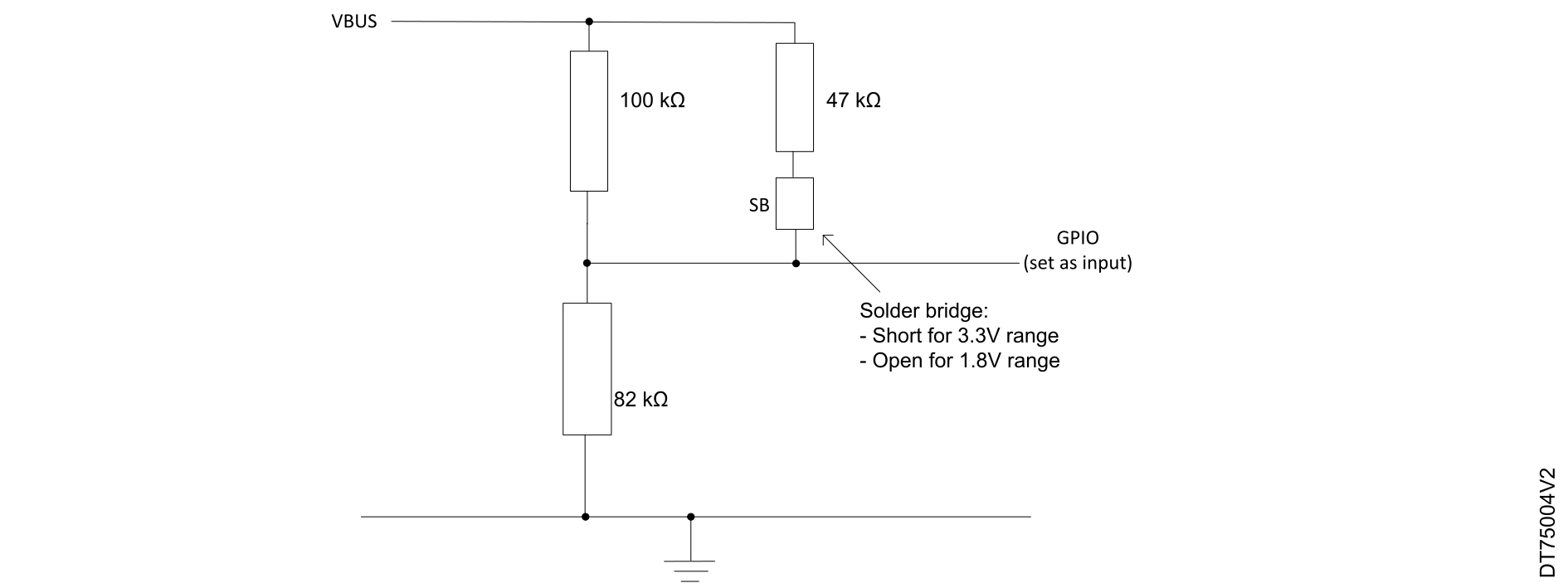
It is also possible to use only three resistors with a solder bridge as shown in Figure 5 Resistor divider supporting both 1.8 and 3.3V ranges.

Figure 5. Resistor divider supporting both 1.8 and 3.3V ranges


MOSFET detector

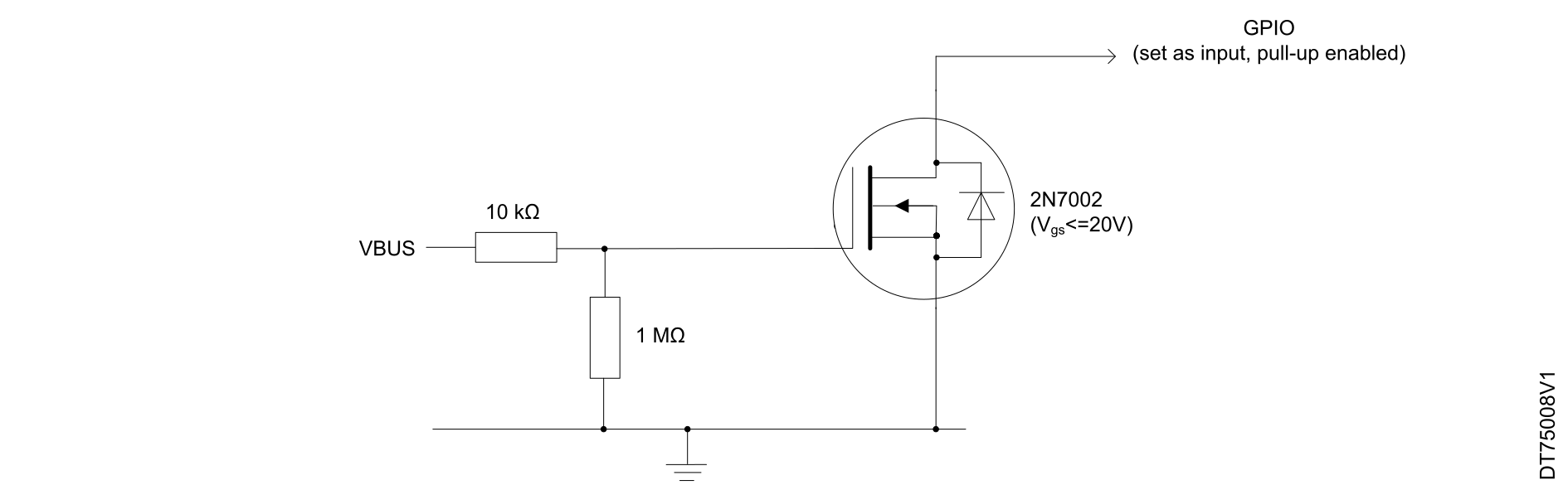
When the GPIO input tolerance is lower, a simple resistor divider is no longer electrically compatible. A simple and cheap way to detect VBUS presence in this case is to resort to an N-channel MOSFET, the recommended device is a 2N7002. Note that this scheme inverts the detection compared with a resistor divider (low level when VBUS is present). See Figure 6 VBUS detection when GPIO max below.

Note:

This solution is recommended when GPIO maximum operating conditions are < VDD+ 3.6 V

Figure 6. VBUS detection when GPIO max


USB FS upstream port

In peripheral mode, the VBUS power is always provided through the cable. The USB FS impedance driver is always managed internally to avoid the need to add external serial resistors on the data line path.

According to the USB specification, there are two main use cases:
  • Self-powered applications: platforms providing their own power supply and acting as an upstream port on the cable insertion. Not allowed, under any condition, to draw any current from the USB interface.
  • Bus-powered applications: a platform supplied only through VBUS and acting as an upstream port.

USB FS upstream port in self-powered applications

To optimize the power consumption on self-powered platforms, only a USB PHY and a controller must be started on the VBUS detection.

It is recommended to implement a resistor bridge (refer to VBUS sensing detection for more details). It is also recommended to use an ESD protection device and to place it as close as possible to the USB connector.

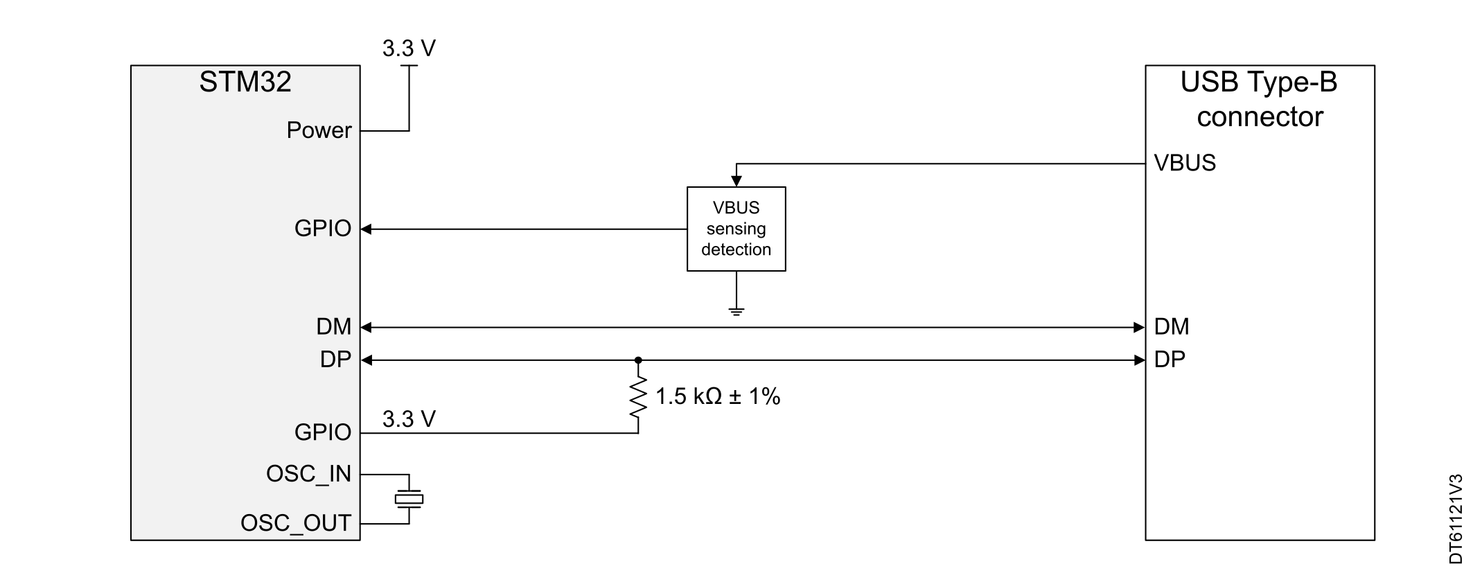
To be compliant with the USB 2.0 full-speed electrical specification, the USB_DP (D+) pin must be pulled up with a 1.5 kΩ resistor to a voltage in the 3.0 to 3.6 V range.

In several STM32 MCUs, the pull-up resistor is already implemented. The user must add this resistor in other STM32 MCUs (refer to the 'Embedded pull-up resistor on USB_DP line' column in AN4879_USB-on-STM32-products.html#id_3644__table_irq_4n2_5fb).
Note:

Since OTG_HS PHY hardware internally behaves similarly for VBUS sensing, the same external resistor approach applies. The difference between FS and HS PHY is basically in data signaling speed, not in VBUS detection logic.

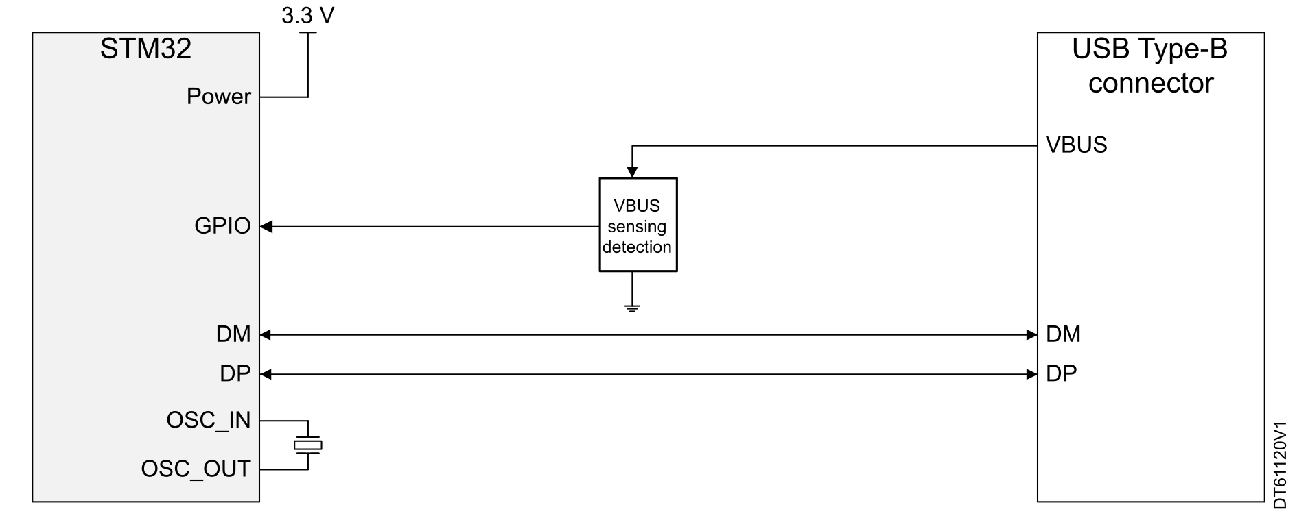
Figure 7. USB FS upstream port with embedded pull-up resistor in self-powered applications


Figure 8. USB FS upstream port without embedded pull-up resistor in self-powered applications


A DP pull-up must be connected only when VBUS is plugged. A GPIO from the MCU is used to drive it after the VBUS detection.

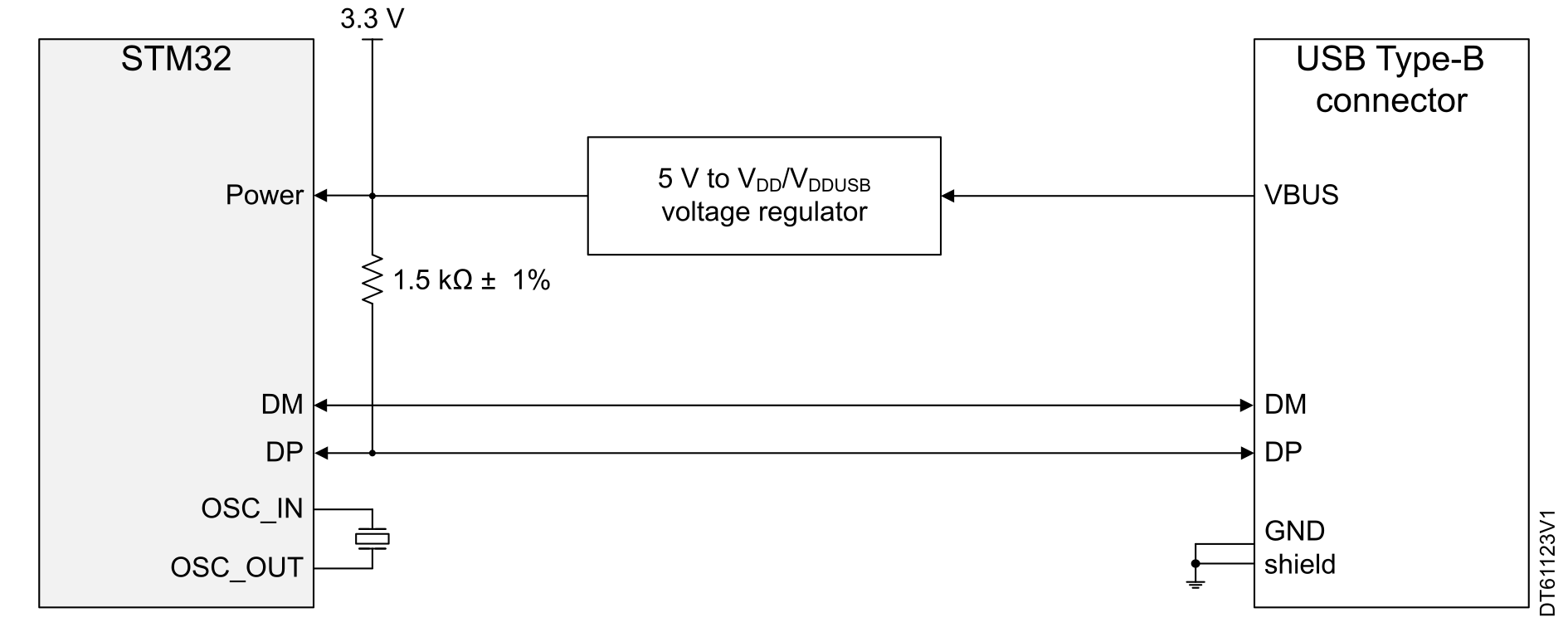
USB FS upstream port in bus-powered applications

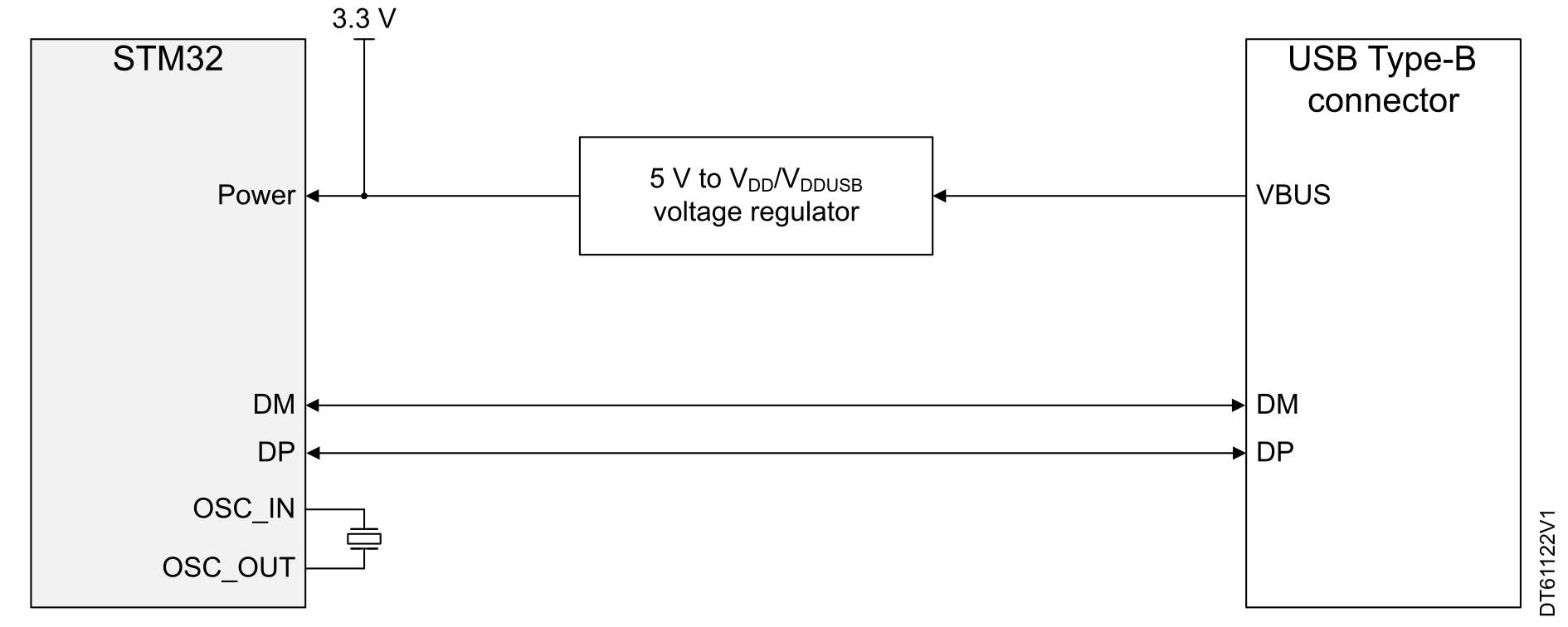
A bus-powered application is an application where the supply comes exclusively from VBUS. In order to keep the host alive and the VBUS available, both the PHY and the controller must always be active.

It is recommended to use an external low-dropout regulator (LDO) to lower the input supply of the MCU (LDO39050PU33R or an equivalent component can be used), and to place the ESD protection chip (if used) as close as possible to the USB connector.
Figure 9. USB FS upstream port with embedded pull-up resistor in bus-powered applications


Figure 10. USB FS upstream port without embedded pull-up resistor in bus-powered applications


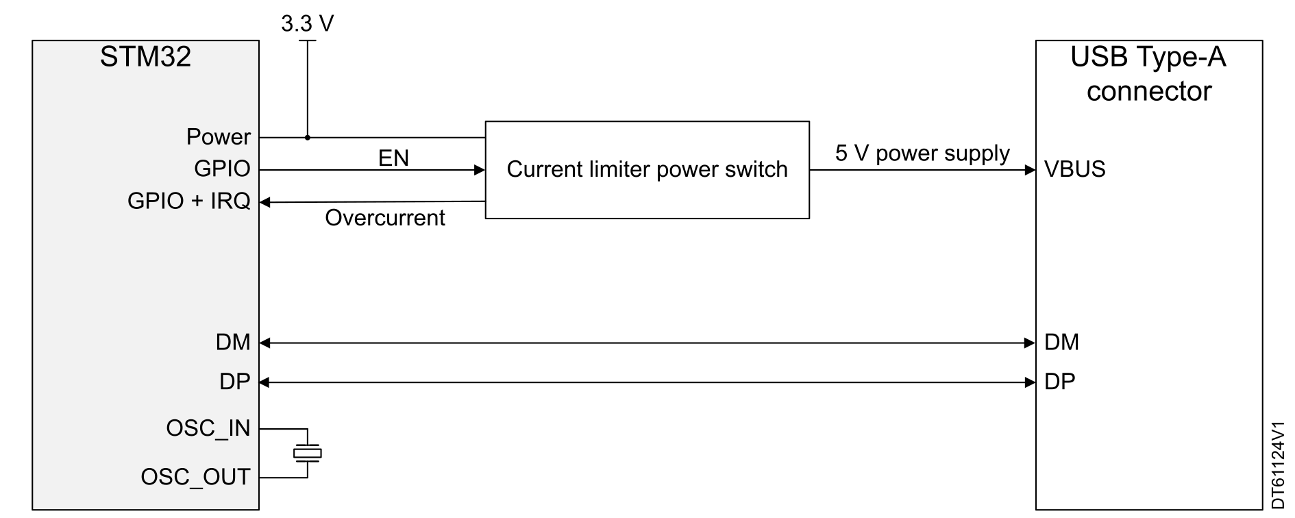
USB FS downstream port

This section describes the implementation for the USB FS downstream port, available on all the STM32 microcontrollers supporting host connection.

As required by the USB specification, if a VBUS overload occurs, it must be indicated to the user. The information regarding a VBUS overload is provided to the STM32 device via a switch with overcurrent protection (STMPS2151STR or equivalent)., as shown in the figure below.

The ESD protection chip, if used, has to be placed as close as possible to the USB connector.
Figure 11. USB FS downstream implementation


OTG applications through embedded PHY

The USB OTG products address scenarios that allow portable devices and non-PC hosts to have the following enhancements:
  • targeted host capability to communicate with a list of selected USB peripherals
  • support for direct connections between OTG devices
  • power saving features to preserve battery life
  • a new pin on a connector, named ID, identifies the USB power role
Consequently, the OTG platforms must include:
  • an STM32 MCU supporting the OTG feature
  • a Micro-AB connector: the USB role is identified through the ID pin
  • a VBUS generation when the OTG device acts as a downstream facing port
  • a VBUS current overflow, both monitoring and acting as a downstream facing port
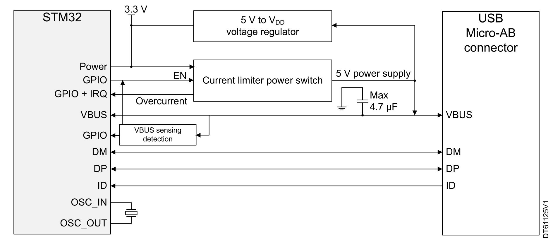
Regarding the figure that is presented below:
  • The OTG specification requires the use of a capacitor (maximum value 4.7 μF) on VBUS.
  • The ESD protection chip, if used, must be placed as close as possible to the USB connector.
  • A power switch (such as STMPS2151STR) is required.
  • When an overcurrent is detected, the information is sent to the STM32 software, which alerts the user about the issue (it is recommended to route VBUS far from DP/DM).
  • The STM32 must always be supplied when the platform is connected as device to a host (in case of dead battery support, the voltage on PA9 must be reduced as explained in VBUS sensing detection).
Figure 12. OTG schematic implementation (dual-mode)


Additional considerations:
  • An external voltage regulator is only needed when building a VBUS powered device.
  • The current limiter is required only if the application has to support a VBUS powered device. A basic power switch can be used if 5 V supply is available on the application board.
  • The ID pin is required in dual role only.
  • The same application can be developed using the OTG_HS in FS mode to achieve enhanced performance thanks to the large Rx/Tx FIFO and to a dedicated DMA controller.