Successive approximation principle
The ADC in STM32G4 Series is based on the successive approximation register principle. This principle is depicted in the figure below:
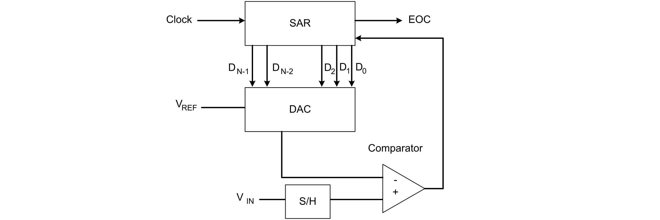
The input voltage (VIN) is sampled by the sample-and-hold block (S/H) (as voltage on sampling capacitor) to have stable voltage during conversion time. This sampled voltage is then compared by the comparator with a known voltage. This known voltage is provided by the DAC that is supplied by the reference voltage VREF.
The DAC digital input is generated by the successive approximation register (SAR) as a digital word. This digital word is generated according to the result from the comparator and is based on the successive approximation principle. The SAR initially generates a word corresponding to a half-voltage range. If the result from the comparator is zero (meaning that input voltage is less than ½ VREF), then, in the second step, the word corresponding ¼ VREF is generated by the SAR . In each approximation step, the SAR adds or subtracts 2n weight according to the current step result from the comparator. After N steps, the SAR generates a final word that is the ADC digital result. The generated analog voltage is close to the measured voltage (with maximum ½ LSB difference).
Maximum ADC speed in successive approximation
The maximum ADC speed is given for the successive approximation principle by the DAC speed and the comparator speed (see Figure 1 ADC operation based on successive approximation principle). In each successive approximation clock cycle, the DAC must set the correct stable analog voltage on its output (with ½ LSB accuracy) and the comparator must provide the result at the end of each cycle.
For example: If the ADC clock is 60 MHz, then each ADC clock cycle takes 1 / 60 MHz = 16 ns. This 16 ns time represents the DAC output stabilization time plus the propagation delay of the comparator.
Switched capacitors
The ADC principle in STM32 MCUs is based on successive approximation where the DAC is based on switched-capacitor network. The capacitor network implementation is technologically acceptable and precise. The advantage of this solution is that the capacitive network works also as sampling capacitor. So there is no need to have one more additional sampling capacitor.
The principle of this implementation is explained in section 1. ADC internal principle of the application note How to get the best ADC accuracy in STM32 microcontrollers (AN2834).
The figure below shows the basic principle of switched-capacitor SAR ADC principle (for a 10-bit ADC).
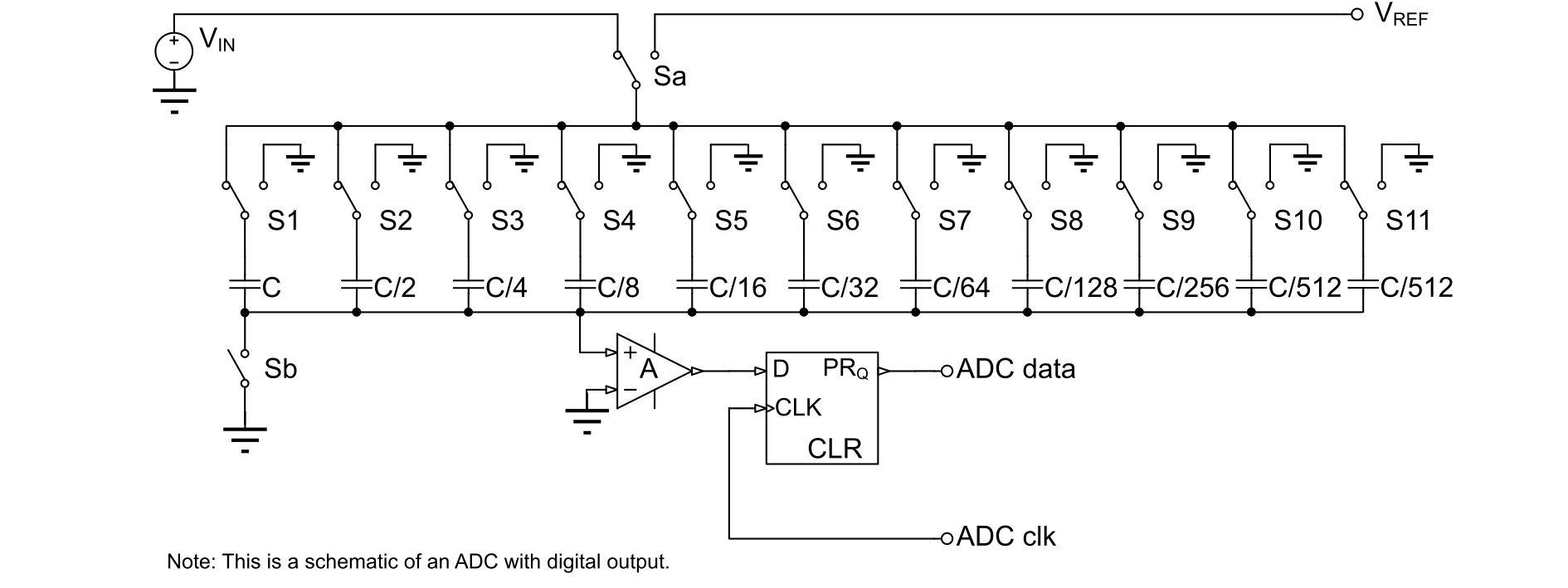
In this figure, the input voltage (VIN) is connected through sampling switch (Sa) to the whole capacitive network that works as sampling capacitor (its charging duration defines the sampling time, Sb is closed). The whole capacitive network is charged to VIN voltage. Then the Sa switches from VIN to VREF and Sb is open. Then the successive approximation is performed: in each clock cycle, the switches S1 to S11 are rearranged and the comparator compares the final voltage. During each S1 to S11 switches rearrangement, there is a charge redistribution between capacitors.
Parasitic components
In each approximation step, the charge redistribution between capacitors is performed. This charge redistribution causes current peaks between capacitors and also from VREF voltage (see Figure 2 Basic schematic of SAR switched-capacitor ADC (10-bit ADC example)). Those current peaks are limited by the parasitic components: resistance and inductance between capacitors and VREF/VSSA voltage.
At the end of each approximation cycle (ADC clock frequency), all currents must be close to zero because the voltage must be stable for comparator comparison. The speed to reach this stable state during charge redistribution is given by all RLC components. The dominant capacity fraction is the capacity of the capacitors network, respectively rearranged sampling capacitor into serial-parallel combination during the approximation (given by configuration of S1 to S11 switches).
The R and L components are parasitic:
- R represents the resistance: dominant is the resistivity of switches S1 to S11 (and on-chip metal paths).
- L represents the inductance of all conductive paths: dominant is the longest conductive path from VREF/VSSA pads to VREF/VSSA pins (bonding wires and on-chip metal paths).
In practice there are attenuated voltage and current oscillations in each approximation step. For correct operation, the amplitude of voltage oscillations (on comparator, respectively on the capacitor network) must decrease below 1 LSB.
The frequency of oscillations is given by LC components and the attenuation is given by RL components. For rapid attenuation, the inductance must be kept at a low value: exponential decrease of oscillations is given by the following formula:
e - R / (2 L) . t (envelope of attenuated oscillations at frequency (2πf)2 = 1 / (LC))
The ADC maximum operating frequency is given by those parasitic RL components.
Note:
A large decoupling capacitor must be connected directly between pins VREF+ and VSSA. This capacitor creates an ideal VREF voltage source (fixed DC voltage without oscillations on this decoupling capacitor).
Application design to reach ADC maximum conversion speed
Decoupling capacitor and PCB design
As mentioned in the previous section, the VREF+ pin must be correctly decoupled.
An appropriate decoupling capacitor must be connected between VREF+ and VSSA pins with a minimum added inductance. Each 1cm of metal path on PCB adds approximately from 6 to 10 nH of inductance. The decoupling capacitor must be placed as close as possible to VREF+ and VSSA pins without through hole connections that may create a loop increasing the inductance.
The placement of the decoupling capacitor must be made on the same layer as VREF+ and VSSA pins. The decoupling capacitor must have a low ESR and a low inductance (for example: ceramic capacitor).
Package selection
The internal parasitic inductance depends on the chip layout and also on the distance between the VREF+/VSSA pads on chip and the VREF+/VSSA pins on the package (bonding wire length).
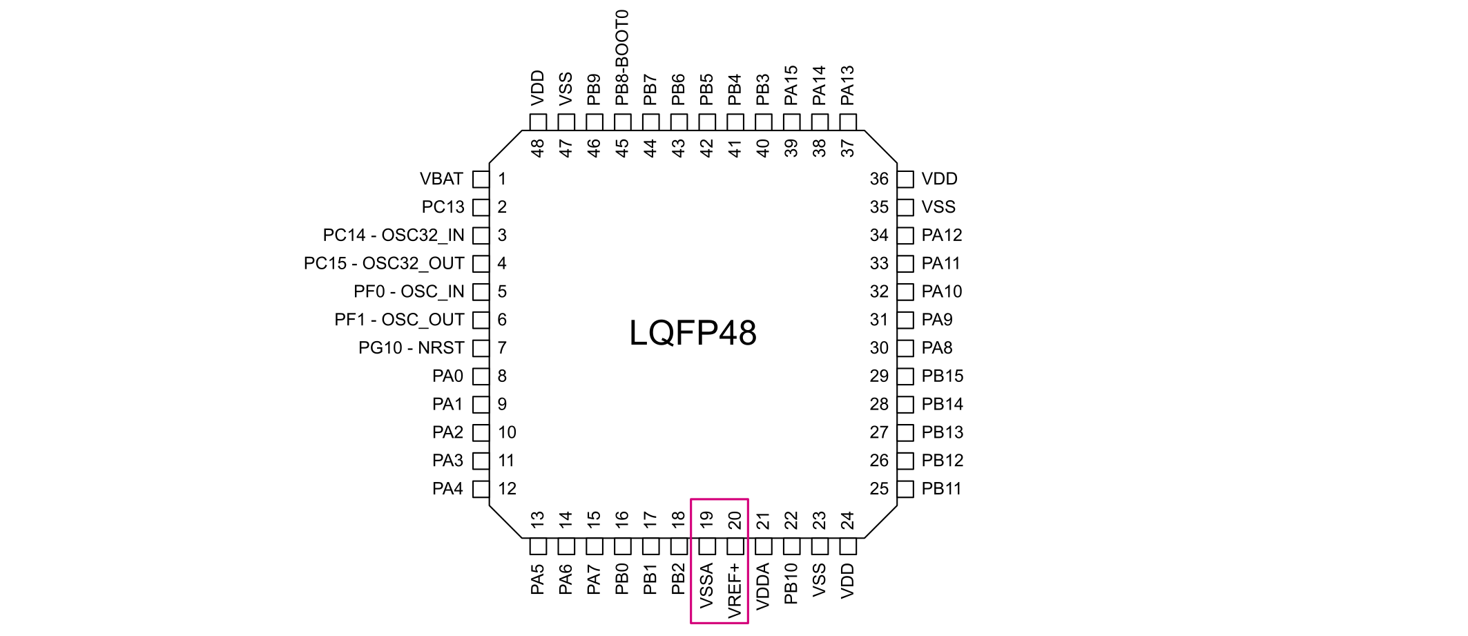
This distance is given by the bonding wires and the pins. The pinout of STM32G4 Series MCUs is designed to have a minimum internal inductance: VREF+ and VSSA pins are adjacent, creating then a minimum current loop and minimizing the internal inductance (see the figure below).
Even though, some packages offer lower distance between chip pads and package pins. For example, the internal inductance is larger on LQFP packages than on UFBGA, UFQFPN or WLCSP packages, due to longer wires from pads to pins.
To decrease even more the inductance on large packages (such as the high-pin count LQFP128) has a VREF+ signal connected by two wires to the two VREF+ pins.
Decrease of ADC clock frequency
If the PCB design is not good enough and if there is an additional external inductance, the oscillations are not attenuated below 1 LSB at the end of the approximation cycle (equal to ADC clock cycle). In this case the ADC may produce DNL errors at high ADC clock frequency.
The solution is to decrease the ADC clock frequency with keeping, if possible, the required final data sampling rate.: slow down each approximation cycle and wait more time for attenuation.
Application example
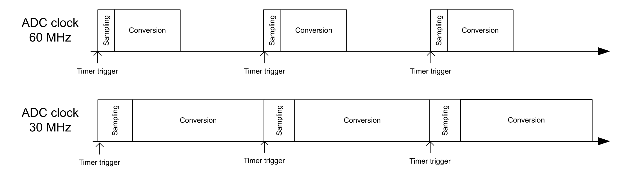
In this example:
- The ADC is triggered by a timer at a 2 MHz trigger frequency ( ADC conversion triggered every 500 ns).
- The ADC clock is 60 MHz.
- The sampling time is 2.5 ADC clock cycle.
- The conversion time is 15 ADC clock cycles (250 ns).
- The sampling rate is 1 / 250 ns = 4 Msps.
The ADC frequency can be decreased down to 30 MHz (each approximation cycle is then two times longer), while keeping the timer trigger frequency at 2 MHz.
STM32G4 multiple ADCs and parallel operations
Parasitic oscillations influences
Up to five ADC instances are implemented in the STM32G4 Series MCUs. More than one ADC is used at one time in the applications, means various ADCs conversions happen at the same time. This ADCs parallel operation may influence the final ADCs results.
The effect of parasitic RLC components to conversion speed is explained in Parasitic components. In case of parallel ADCs operation, all the ADCs use the same VREF voltage. The schematic diagram in Figure 2 Basic schematic of SAR switched-capacitor ADC (10-bit ADC example) is therefore multiplied but the VREF voltage remains common for all ADCs. There are more capacitors networks connected in parallel to VREF. More capacity change in each approximation step causes higher current peaks from VREF and the internal oscillations have then higher amplitude. The frequency of oscillations decreases due to larger capacity connected to VREF.
Due to all those effects, the attenuation reaches 1 LSB level later and the maximum ADC frequency of all parallel operating ADCs is lower than in case of only one ADC. If the ADCs clock is kept high, the attenuation does not decrease below 1 LSB level and the ADCs produce DNL errors. There is also an interference between the ADCs: one ADC influences another ADC result. This influence depends on the synchronization between the ADCs: when a given ADC starts an approximation regarding to another ADC. The ADC frequency must be decreased to keep the ADCs results accurate (each approximation cycle is extended).
Optimizations for multiple-ADC operation
The suggestions for the design of an application using multiple-ADC operation are the same as for a single ADC (refer to Application design to reach ADC maximum conversion speed): good VREF+/VSSA pins decoupling, correct VSSA grounding.
For multiple-ADC operation, all the effects of the internal oscillations and charging currents from VREF are cumulated (from all used ADCs). A correct PCB design is therefore very important: take care of the decoupling of VREF+ pin and the correct grounding layout, because there are relatively high current peaks on the VREF+ pin.
Note:
Unstable voltage on pin VREF+ can influence the DAC performance because the VREF+ pin provides reference voltage for the DAC.