Limitation description
This limitation is described in the errata sheets of the STM32G4 Series MCUs. More details and possible workarounds are detailed below.
Each ADC has an input multiplexer that performs the selection of a given channel: there are sets of analog switches between the ADC input and a given pin on the package. The Sa sampling switch (see Figure 2 Basic schematic of SAR switched-capacitor ADC (10-bit ADC example)) is implemented behind the multiplexer. Sa is switched on during sampling time (initiated by the trigger). During the successive approximation, Sa is open to isolate the capacitors network from the analog input. The multiplexer is switched to the next programmed channel in the middle of the successive approximation (in case of scan mode). If the ADC is used in single mode or at the end of the scan sequence, the multiplexer is switched to the internal channel (Channel 31).
The multiplexer switching from the current channel to the following channel generates some noise that may influence the successive approximation currently in progress (especially the bit under evaluation in the successive approximation sequence). This may also impact the DNL error of any ADC currently converting.
The worst case is when various ADCs operates synchronously and their input multiplexers switch to the next channel at the same clock cycle (usually the case as all ADCs are programmed with the same parameters and triggered by the same trigger). In this case, the noise is cumulated and the DNL error of the ADC results is maximal.
Workaround
This workaround is based on disabling the input multiplexer switch during the successive approximation.
The input multiplexer switch is not performed in the following cases:
- in continuous conversions for the same channel
Continuous conversions are performed on the same channel and the input multiplexer is kept switched on the given selected channel (except for the final conversion).
- in bulb mode for the same channel
The input multiplexer is kept switched on the selected channel (and does not switch to internal channel) because the sampling phase starts immediately after finishing conversion from the same selected channel.
- in scan sequence if the next channel number is the same as current channel number
The multiplexer switches to the following channel in the middle of the conversion, but no switch is performed if the following channel number is the same as current channel .
The above cases can be used as workaround to solve switching problem. In single channel applications (only one channel per ADC is used), the 'bulb mode for the same channel' use-case is appropriate. In multiple channels applications (various channels per ADC are used), the last use-case is better.
In the last use-case, the original channel scan sequence must be modified that each channel is doubled into pairs in the scan sequence. The correct results are taken only from the first sample of the pair. This solution leads to decrease the effective sampling data rate to one half (each second conversion is thrown). This case offers also a solution if various ADCs are operating together in synchronous operation. In asynchronous ADCs operation, the channel switching noise may influence another ADC as the channel switching is not synchronized among ADCs.
Optimized channels sequence
For some applications, the proposed workarounds are not suitable. For example, a high data rate is required and doubling each channel in scan sequence impacts too much data rate. In this case the scanned channel sequence can be optimized regarding the channel numbers order.
The noise level generated by the multiplexer channel switch depends on the channel numbers used, especially on the change between current channel number and the following channel number. The generated noise level is proportional to the number of bits changed in the channel number (in case of channel change).
Each number (for example Channel 6) has a binary representation (0110 in the example). If there is a change to the next number (for example to Channel 15 with binary representation 1111), the generated noise is proportional to the number of changed bits in this number (2 bits changed from Ch 6 to Ch 15: 0110 to 1111). Those changed bits represents the Hamming distance. An optimum channels sequence represents a Gray code sequence. In a Gray code sequence, only one bit is changed between each number change.
Example
For numbers 0-15, the Gray code sequence in binary representation is the following: 0000 to 0001 to 0011 to 0010 to 0110 to 0111 to 0101 to 0100 to 1100 to 1101 to 1111 to 1110 to 1010 to 1011 to 1001 to 1000.
The ADC channels numbers must be carefully selected for the scan sequence, to minimize the impact of this ADC limitation.
When no scan mode is used (channel selected by software before each conversion), the channel switching is performed to the internal channel (in the middle of the conversion). The internal channel is Channel 31 in the ADCs of the STM32G4 Series MCUs. In this case, the workaround with bulb mode only is recommended: optimization with Gray code to number 31 is possible only from number 15: 01111 to 11111). The workaround with bulb mode completely removes this ADC limitation.
Minimize the ADC errors
General rules
The application note How to get the best ADC accuracy in STM32 microcontrollers (AN2834) describes the general rules, methods and recommendations for correct design of applications using ADCs. Refer to this document to design properly any application with STM32G4 Series MCU ADCs.
Specific recommendations
The ADCs in STM32G4 Series devices have some specific properties for which the following additional recommendations are defined:
- Reference voltage on VREF+ pin can be also driven from VREFBUFF (internal reference voltage used on VREF+ pin):
- Use recommended decoupling capacitor on VREF+ pin: 1 μF + 100 nF. Place this capacitor directly between VREF+ and VSSA pins.
- Take care of the external load connected to VREF+ pin. Driving capability of VREFBUFF is 6.5 mA, that covers also the internal ADCs and DACs consumptions from VREF+ pin. If the application uses more ADCs and DACs, the external driving capability from VREF+ pin decreases proportionally (see the STM32G4 Series datasheets for ADC and DAC current consumptions from VREF+).
- VSSA and VSS grounding:
- The VSSA pin must be connected as close as possible to the VSS pin. The VSSA pin is used as analog supply (together with VDDA pin) and also as ground reference for VREF+ voltage (VSSA pad is internally double bonded with VREF- pad).
- The PCB design must use a large ground plate for VSS ground and connect VSSA pin directly to this VSS ground plate. If a specific voltage source is used for VREF+ (or VDDA), connect this voltage source directly to VREF+/VSSA or VDDA/VSSA pins.
- Filtering of analog supply voltages:
- Avoid to use of larger inductors as filters for VSSA or VREF+ pins. The inductor together with the decoupling capacitor create an LC filter that operates correctly only if its load is stable (like some resistance on the LC filter output). It filters correctly the input voltage fluctuations. If the LC filter load generates current peaks (like current peaks from VREF+ or VDDA pin), this fast transient current peak can lead to attenuated oscillations of this LC filter at its resonant frequency. In fact, the current peak decreases the voltage on the decoupling capacitor and, because the inductor inhibits large current changes, the capacitor is charged back slowly and the LC circuit may oscillate. These voltage oscillations are present on the decoupling capacitor and therefore, the VREF+ or VDDA voltage is influenced. The oscillations on VREF+ or VDDA pin are attenuated after a relative long time (when the current peak disappears) and may influence the VREF+ and VDDA voltages in later critical times.
- In some designs, the high frequency inductor (or better say choke) must be used to filter very high noise from the power supply (if really present). In parallel to this choke footprint, it is recommended to design the solder bridge that can short the choke in case of problems with VREF+ or VDDA voltage stability (see the example in the figure below). The ferrite choke must be properly selected to filter very high frequencies (relative to current supply peaks frequency) and their impedance character at high frequencies must be more resistive than inductive (high-frequency losses in the ferrite core).
Figure 5. Example of designing solder bridges (SB8, SB10) in parallel to chokes (L1, L2) on analog supply voltages 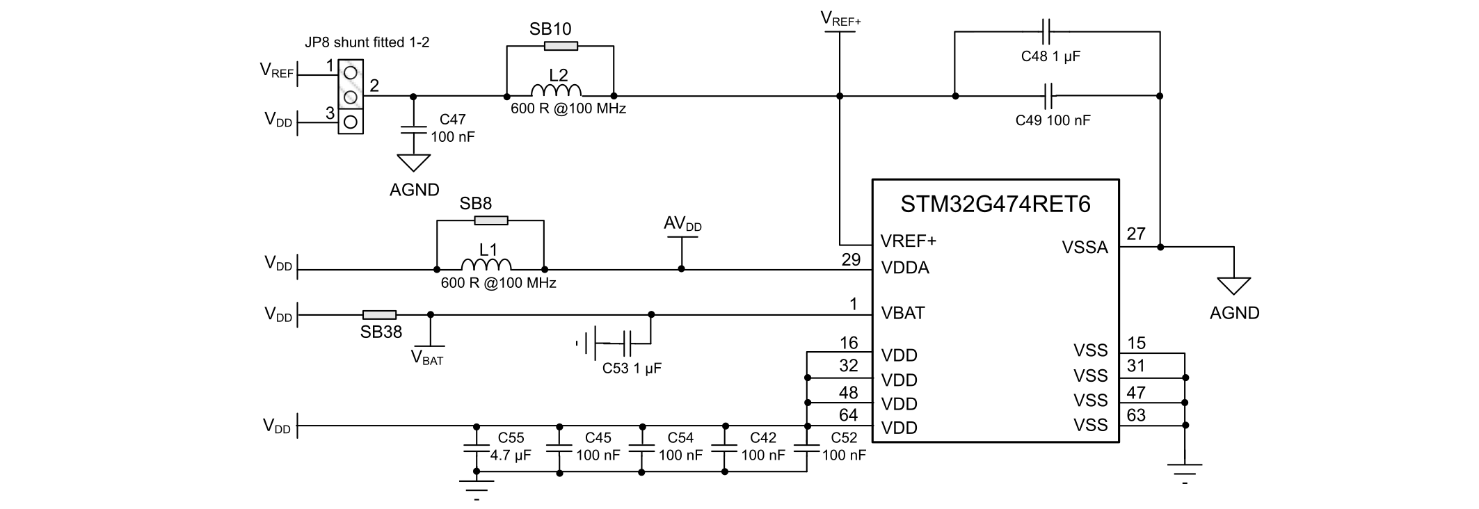
- Signal source driving properties knowledge regarding to ADC input properties:
- The signal source impedance value must be known to correctly design the ADC sampling time. If the signal source has higher impedance, longer sampling times must be used to charge properly the sampling capacitor (see STM32G4 Series devices datasheets for recommended ADC sampling times for various external source impedance). The use of longer sampling time leads to decrease the maximum ADC data rate. For very fast data rate, the use of signal source with low impedance is recommended.
- To decrease the signal source impedance, an analog buffer can be used as ADC signal source (for example OPAMP in the follower mode). The speed of this analog buffer (slew rate and frequency bandwidth) must be known to correctly program the ADC sampling time. At the beginning of the ADC sampling phase, the discharged sampling capacitor is connected to the analog buffer (OPAMP) output. The voltage on the OPAMP output is zero at this moment (discharged sampling capacitor at OPAMP output). Then the OPAMP (thanks to its feedback) starts compensating this unbalance by increasing the output driving and charging the sampling capacitor. The speed of this OPAMP driving increase depends on the OPAMP speed (propagation of the OPAMP input change to the OPAMP output change). In the example of the OPAMP embedded in STM32G4 Series devices: The OPAMP has a frequency bandwidth of 13 MHz. A first estimation of the propagation delay is 1 / 13 MHz = around 77 ns. The sampling capacitor must then be charged by the OPAMP to 1 LSB accuracy. The recommended ADC sampling time to read the embedded OPAMP output by ADC is 200 ns (see the datasheet). If the ADC clock is for example 60 MHz, the sampling time must be programmed to more than 200 ns x 60 MHz = 12 clock cycles (leading to program sampling time to 12.5 ADC clock cycles, bits SMP[2:0] = 010). The final data rate is then 60 MHz / (12.5 + 12.5) = 2.4 Msps (maximum data rate while using the embedded OPAMP as buffer for ADC).
- For measurement of signal sources with very high impedance, refer to section 3.4 High impedance source measurement of the application note How to get the best ADC accuracy in STM32 microcontrollers (AN2834), where some methods for high-impedance source measurement and design calculation for practical implementation are detailed.
Revision history
| Date | Version | Changes |
|---|---|---|
| 14-Jun-2019 | 1 | Initial release. |
| 15-Oct-2019 | 2 | Updated Table 1 ADC features on STM32G4 Series. |