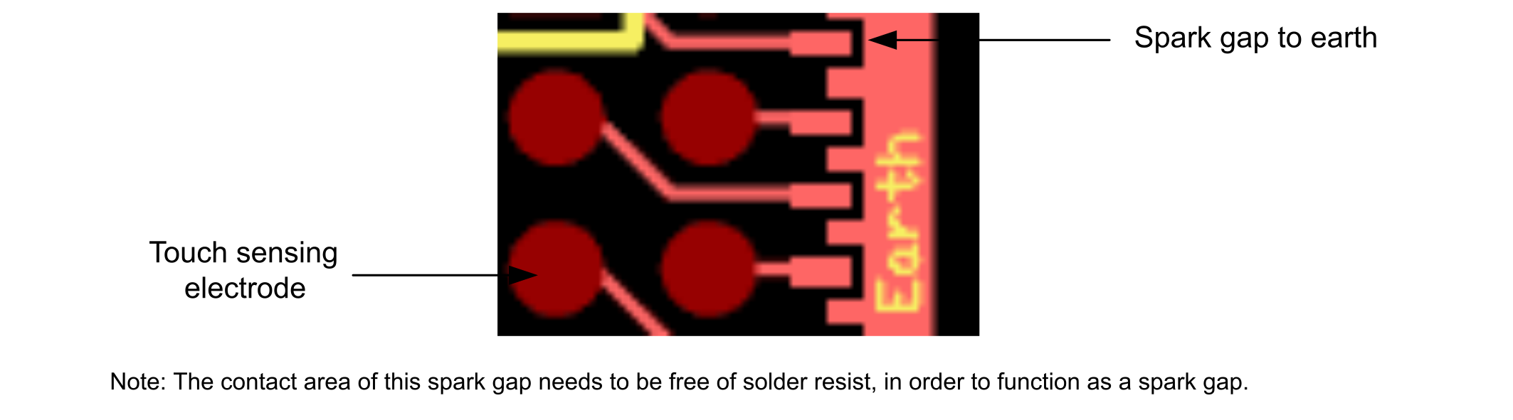
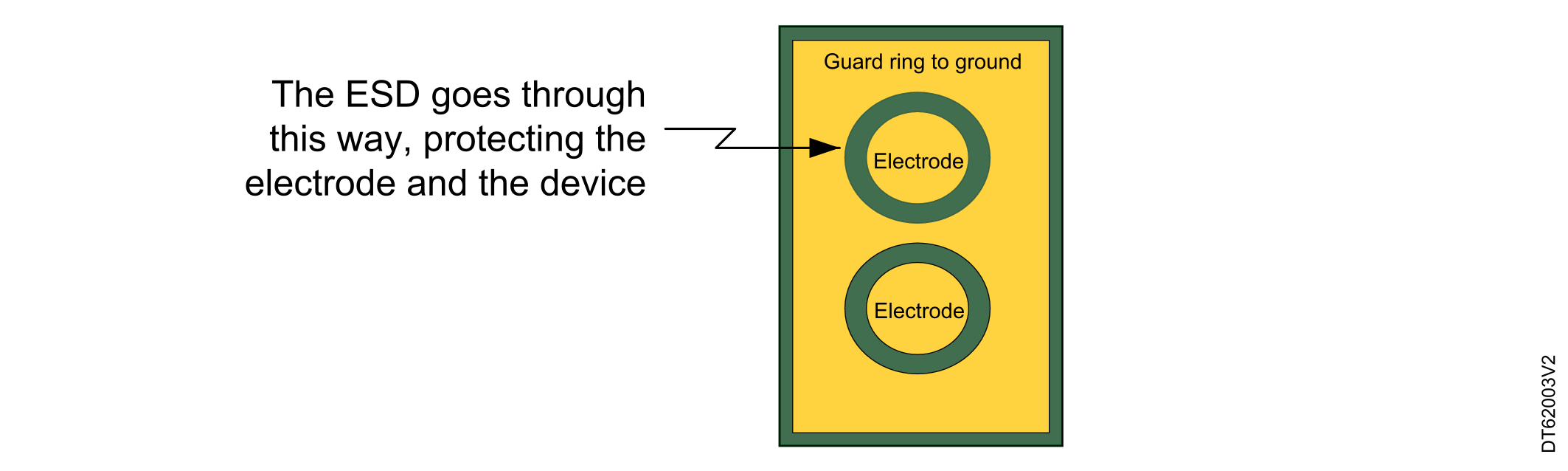
Input/output lines that are susceptible to ESD stress are sometimes protected by adding external diodes that shunt the high energy of the ESD stress before it can reach the device input pin. These diodes may either pass the current to the power-supply rails or may internally dissipate the unwanted power. External diodes are similar to the diodes built into a device (internal diodes) for protection but they are designed differently. External diodes have the following significant advantages:
- They can switch faster and at a lower excursion voltage than the internal diodes of the device.
- They can have much better connections to the supply rails and can carry more power.
The effects of external diodes on circuit operation are different from internal diodes, because the connections used internally cannot be achieved with external devices.
The following types of protection diode are typically used against ESD stress:
- Transient voltage suppression (TVS) diodes can be placed between an input signal and ground. In this configuration, the diode protects the CMOS input by reverse conduction whenever its voltage rises above the specified diode breakdown voltage. Negative ESD excursions are shunted to ground through normal diode action.
- Diode pairs (such as Schottky diodes, with lower forward voltage drop) are placed between the input line and the power and ground rails. These devices protect the CMOS input by normal diode conduction whenever the input line voltage moves outside the range of the power supply rails.
For touch sensing, an additional Schottky diode (like ST BAS70), can be used to improve conducted noise immunity (IEC61000-4-6). ESD, in this case, is not the main concern.
Diodes placed on capacitive sensed lines present the same problems to capacitive sensing circuits as they do with any analog circuit input: they can be highly capacitive (over 100 pF) and leaky. Some Schottky pairs leak over 20 µA; some avalanche diodes leak over 1 mA when operated near their reverse-standoff voltage (generating significant noise voltage as well).
Although these given numbers are for the least suitable devices, the most commonly-used schottky and TVS diodes have parasitic parameters that make them unacceptable for use in capacitive sensing applications. If the diode circuit can be designed to add only a very small amount of additional capacitance, capacitance sensing solutions can be adjusted to match.
Compensation mechanisms are usually built into the touch sensing device for adaptation to the naturally-occurring changes in capacitance that result from environmental changes. However, leakage and bulk capacitance can create problems for any sort of capacitive sensing method, some more than others.
External diodes with high reverse leakage make the test capacitance look larger because their leakage drains test current from the circuit. This disappearing test current (which should fill the capacitance under test) has no dV/dt effect on the test load.
As diode leakage currents approach the level of the test current, the apparent load capacitance approaches infinity. Also, the amount of current required to detect a 0.1 pF change in capacitance is less than 20 pA, many orders of magnitude less than the leakage current for some protection diodes. For this reason, where external diodes must be used, it is essential to specify devices with extremely low reverse leakage.
The ST ESD protection diodes are designed to resist multiple ESD stresses. Their low capacitance (1 pF) and low leakage (less than 100 nA) reduce the problems encountered with Schottky protection diodes. The bidirectional protection ESDAXLC6 diode, with even lower capacitance (0.5 pF) can be used instead of the ESDAULC6 diode to prevent the occurrence of negative and positive pulses.