AN4277 · Application noteHow to use PWM shutdown for motor control and digital power conversion on STM32 MCUs
Download .pdfOpen in the full document

Examples

Examples

Table 5 Scenarios of PWM output status in response to internal/external break events shows the PWM output status for TIMx (where x = 1, 8, 20, 15, 16, 17) in response to internal/external break events.

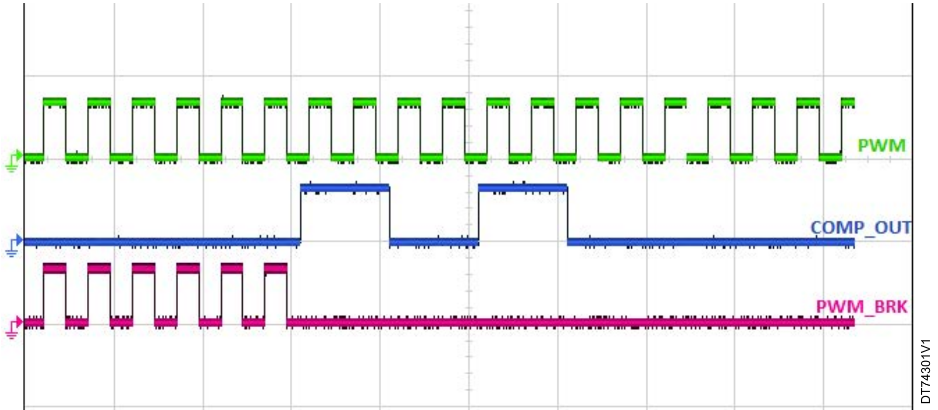
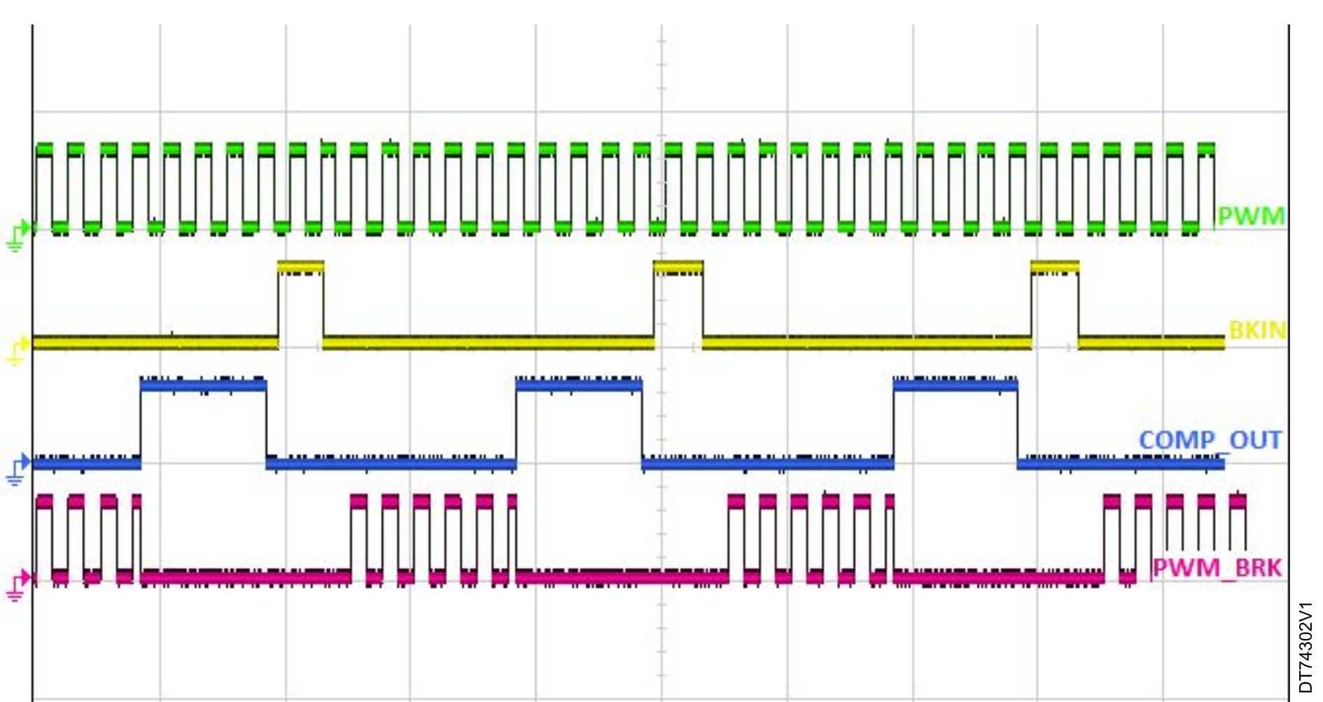
In the following waveforms:

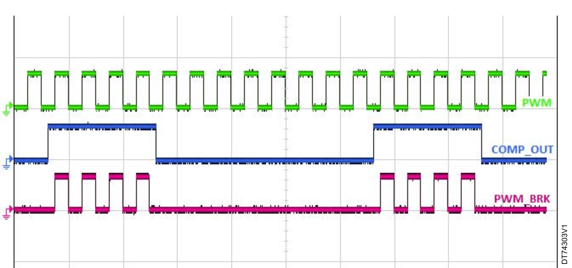
  • The PWM signal is the reference waveform (internal signal, before BRK protection).
  • The COMP_OUT signal represents the BRK input signal, in our case it is the comparator output.
  • The BIN signal is the input signal on BKIN.
  • The PWM_BRK signal is the resulting PWM signal on the timer output after break detection.
Table 5. Scenarios of PWM output status in response to internal/external break eventsColor legend: green = PWM signal, blue = COMP_OUT signal, yellow = BKIN signal, purple = PWM_BRK signal.
ConfigurationProgrammed polarityResult
Comparator 1 output is connected internally to TIM1 BRK_ACTH and TIM1 BKIN alternate function is disabled.HighThe PWM generation is stopped when the comparator output is at the high level, as shown in the following screenshot:

Comparator 1 output is connected internally to TIM1 BRK_ACTH and TIM1 BKIN alternate function is enabled.

High/LowThe break input signal is an OR between the signal on BKIN and the comparator output. The following screenshot shows an example (polarity = High):

Note:

To show the effect of the two break sources, the bit AOE in the BDTR register is set, allowing to restart the PWM at the next update event.

Comparator 4 output is connected internally to TIM1 BRK and the filter is not configured.LowThe PWM signal is stopped during the break signal low level, as shown in the following screenshot:

Comparator 4 output is connected internally to TIM1 BRK and the filter is configured.High

During the window defined by the filter duration, the break event has no impact on the PWM generation even if the break condition is verified.

This is the case of the following example (screenshot) where the PWM signal is generated normally when the break signal is at a high level during the window defined by the filter.
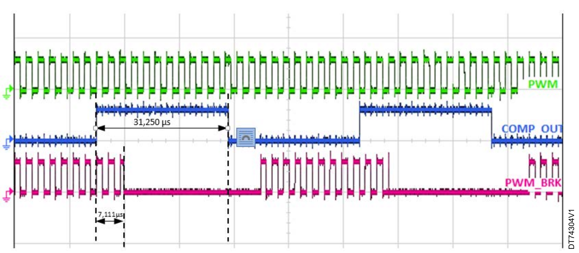
  • The filter duration is 7.111 µs (BKF = 1111b, filter duration is (32*8/fDTS), fDTS = 36 MHz).
  • The comparator output high level duration is 7.111 µs.


Break function used for overcurrent protection

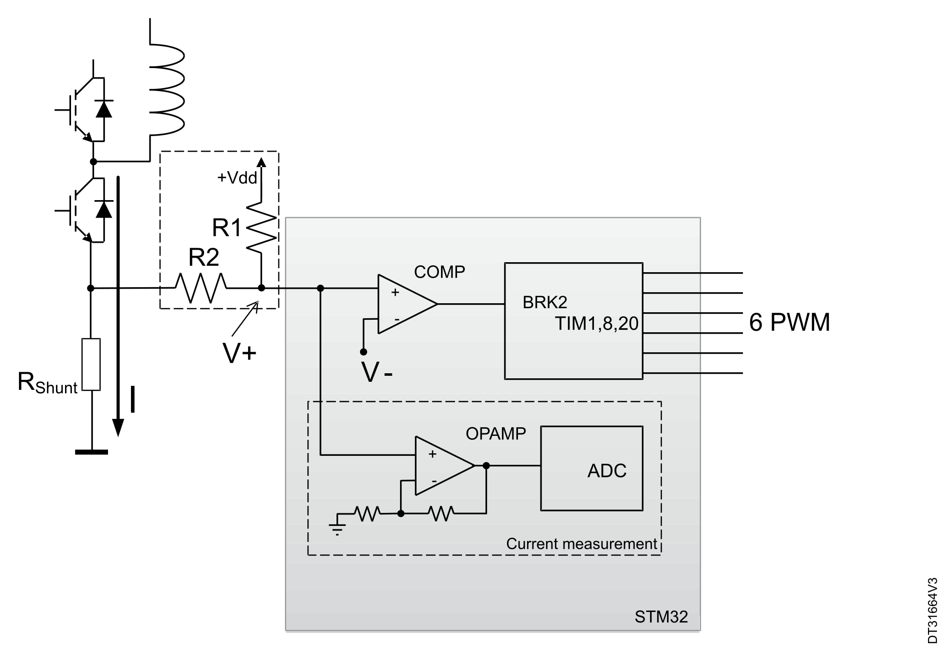
The STM32F3 and STM32G4 series microcontroller embeds a set of peripherals designed to resolve common motor control issues while reducing the number of required external components. This section describes how to use these peripherals to implement overcurrent protection. Figure 10 Overcurrent protection network implementation block diagram shows the overcurrent protection network that can be implemented using the internal resources of the MCU.

Figure 10. Overcurrent protection network implementation block diagram


The principle of this overcurrent protection mechanism can be summarized as follows:

  • The phase current of the motor flows in the power transistor of the inverter bridge and passes through the shunt resistor (RShunt) producing a voltage drop (V+).
  • This voltage drop is compared with a threshold (V-) defining the maximum admissible current.
  • If the threshold is exceeded, a break signal stops the PWM generation putting the system in a safe state.

All of these actions can be performed using the internal resources of the STM32 and, in particular, the embedded comparators and advanced timer break function (BRK2). In the basic implementation, the only external component required is the shunt resistor that must be sized depending on the current to be monitored and the shunt resistor power rating.

The two dotted line boxes in Figure 10 Overcurrent protection network implementation block diagram show the components required to measure current:

  • The R1/R2 resistive network to add an offset necessary to measure AC currents.
  • An operational amplifier with a built-in gain setting network.

The amplification network can be implemented externally for specific use cases where the built-in gain settings are not adequate.

Break function used for overvoltage protection

Figure 11 Overvoltage protection network block diagram shows the overvoltage protection network that can be implemented using the internal resources of many STM32 MCUs.

Figure 11. Overvoltage protection network block diagram


In this case, the principle is similar to the one described in Break function used for overcurrent protection :

  • A resistive voltage divider provides a signal proportional to the bus voltage.
  • This reading is compared to an overvoltage threshold to generate a fault signal. See also: How to use the DAC to define thresholds.
  • If the threshold is exceeded, a break signal stops the PWM generation putting the system in a safe state.

As mentioned before, these actions can be performed automatically using the internal comparator. In this case, it is possible to use the second break functionality (BRK) of the advanced timer to differentiate the action to perform on the PWM signals in case of an overcurrent.

In the basic implementation, the only external component required is the voltage divider, which must be sized depending on the bus voltage range requested by the target application, so that it never exceeds the MCU’s input maximum admissible voltage level.

The dotted line box in Figure 11 Overvoltage protection network block diagram shows the components required for the bus voltage measurement. In this case, amplifying the signal V+ is usually not required (the resistive divider is adjusted for full-range reading), so this signal is fed directly to the analog-to-digital converter.

Using an external emergency signal together with the internal comparator

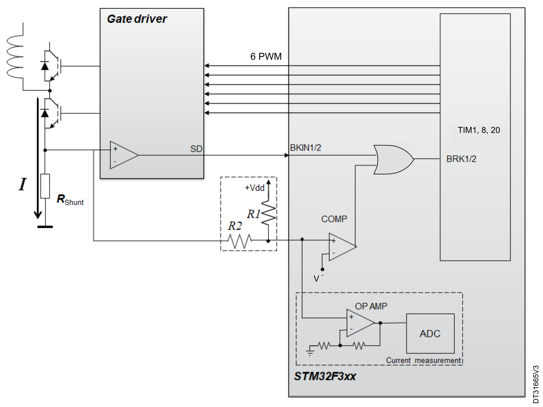
Commonly in MC applications, gate driver ICs, such as ST’s L639x family or intelligent power modules (IPMs) - such as ST’s SLLIMM (small low-loss intelligent molded module) family - have integrated comparators that can protect the inverter (ST’s smart shutdown function) while sending an error signal to the microcontroller.

This section shows the possibility to combine these two concepts, as shown in , as to enhance by redundancy the functional safety offered by the “break function”.

A first option is when the break function is triggered by internal comparators output only: the error signal coming from ICs or IPMs must not be connected to the microcontroller, thus saving the pin. The configuration to set in this case is summarized in the following table.

Table 6. Comparator output connected internally to break inputs
DescriptionRegisterBitConfiguration(1)
TIM1/8/20 BRK_ACTH/BRK/BRK2 polarityTIMx_BDTRBKP or BK2P1 (active high)
Comparator output polarityCOMPx_CSRCOMPxPOL0 (not inverted), comparators input connected as shown in previous sections
TIM1/8/20 BKIN and BKIN2 AFGPIOxAFRL or GPIOxAFRH-AF is not enabled on BKIN1/2 related pins
TIM1/8/20 BRK and BRK2 enableTIMX_BDTRBKE or BK2E1
COMPx out selectionCOMPx_CSRCOMPxOUTSEL

0001: TIM1 BRK or TIM1 BRK_ACTH(2)
0010: TIM1 BRK2
0011: TIM8 BRK or TIM8 BRK_ACTH(3)
0100: TIM8 BRK2
0101: TIM1 BRK2 + TIM8 BRK2
1100: TIM20 BRK or TIM20 BRK_ACTH(4)
1101: TIM20 BRK2
1110: TIM1 BRK2 + TIM8 BRK2 + TIM20 BRK2

On the contrary, the user may prefer to make use of the external error signal in conjunction with the internal one: the result is an OR between the two. Depending on the external comparator logic, the possible configurations to write are summarized in the following tables.

Table 7. Comparator output connected externally to break inputs, with low break polarity
DescriptionRegisterBitConfiguration
TIM1/8/20 BRK polarityTIMx_BDTRBKP0 (active low), it means that the external signal goes low during the fault
Comparator output polarityCOMPx_CSRCOMPxPOL0 (not inverted), comparators input connected as shown in previous sections
TIM1/8/20 BKIN AFGPIOxAFRL or GPIOxAFRH-AF enabled on BKIN pin selected among available
TIM1/8/20 BRK enableTIMX_BDTRBKE1
COMPx out selectionCOMPx_CSRCOMPxOUTSEL

0001: TIM1 BRK
0011: TIM8 BRK
1100: TIM20 BRK

Table 8. Comparator output connected externally to break inputs, with high break polarity
DescriptionRegisterBitConfiguration
TIM1/8/20 BRK/BRK2 polarityTIMx_BDTRBKP or BK2P1 (active high), it means that the external signal goes high during the fault
Comparator output polarityCOMPx_CSRCOMPxPOL0 (not inverted), comparators input connected as shown in previous sections
TIM1/8/20 BKIN/BKIN2 AFGPIOxAFRL or GPIOxAFRH-AF enabled on BKIN/BKIN2 pin selected among available
TIM1/8/20 BRK/BRK2 enableTIMX_BDTRBKEor BK2E1
COMPx out selectionCOMPx_CSRCOMPxOUTSEL

0001: TIM1 BRK
0010: TIM1 BRK2
0011: TIM8 BRK
0100: TIM8 BRK2
0101: TIM1 BRK2 + TIM8 BRK2
1100: TIM20 BRK
1101: TIM20 BRK2
1110: TIM1 BRK2 + TIM8 BRK2 + TIM20 BRK2

The comparators output can be optionally enabled as an alternate function on the related GPIO pin, in push-pull or open-drain mode, for signaling to other devices or for debugging purposes.

Figure 12. Combining external and internal protection concept


1 Some newer STM32 series, such as STM32U5 abandoned the use of BRK_ACTH identifier using name system level or internal fault instead. The functionality remains analogous.
2 TIM1 BRK in case of COMP4 and COMP7, or TIM1 BRK_ACTH in case of COMPx, x = 1, 2, 3, 5, and 6.
3 TIM8 BRK in case of COMP4 and COMP7, or TIM8 BRK_ACTH in case of COMPx, x = 1, 2, 3, 5, and 6.
4 TIM20 BRK in case of COMP4 and COMP7, or TIM20 BRK_ACTH in case of COMPx, x= 1, 2, 3, 5, and 6.