AN4296 · Application noteUse STM32F3/STM32G4 CCM SRAM with IAR Embedded Workbench®, Keil® MDK-ARM, STMicroelectronics STM32CubeIDE, and other GNU-based toolchains
Download .pdfOpen in the full document

Purpose

Purpose

The CCM SRAM is tightly coupled with the Arm® Cortex® core, to execute the code at the maximum system clock frequency without any wait-state penalty. This also brings a significant decrease of the critical task execution time, compared to code execution from flash memory.

The CCM SRAM is typically used for real-time and computation intensive routines, like the following:

  • Digital power conversion control loops (switch-mode power supplies, lighting)
  • Field-oriented 3-phase motor control
  • Real-time DSP (digital signal processing) tasks

When the code is located in CCM SRAM and data stored in the regular SRAM, the Cortex®‑M4 core is in the optimum Harvard configuration. A dedicated zero-wait-state memory is connected to each of its I-bus and D-bus (see the figures below) and can thus perform at 1.25 DMIPS/MHz, with a deterministic performance of 90 DMIPS in STM32F3 and 213 DMIPS in STM32G4. This also guarantees a minimal latency if the interrupt service routines are placed in the CCM SRAM.
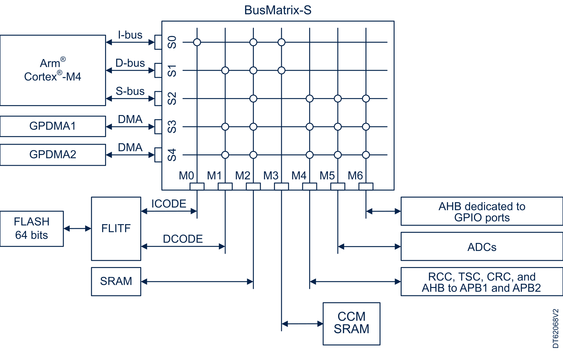
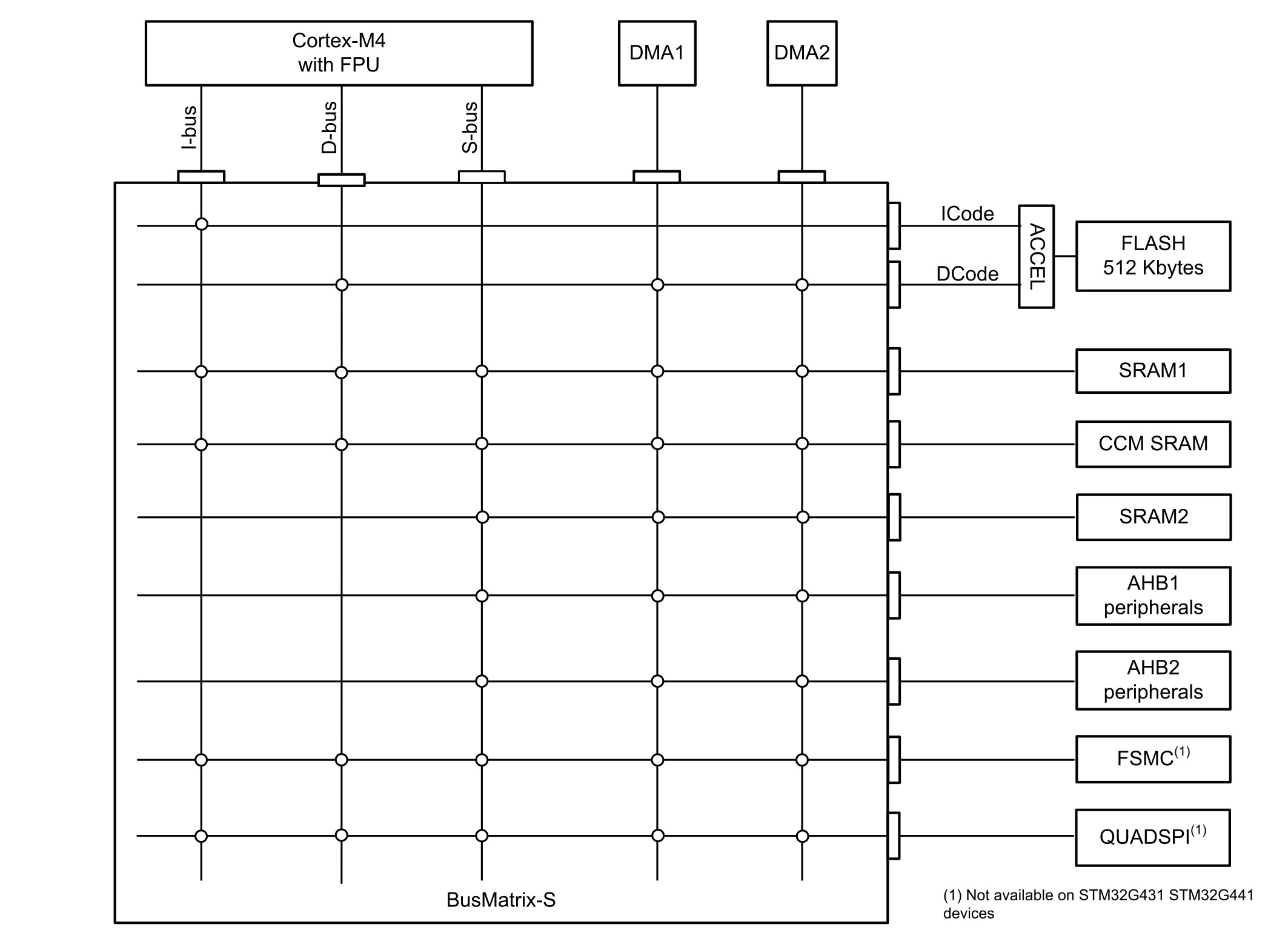
Figure 1. STM32F3 device system architecture
Figure 2. STM32G4 device system architecture

Example

A benchmark between the STM32F103 and STM32F303 microcontrollers using the STMicroelectronics MC library V3.4 shows that, in case of single motor control using three-shunt algorithm, the field-oriented control (FOC) total execution time for STM32F303 is 16.97 μs compared to 21.3 μs for the STM32F103 (see the note below), with FOC core and sensorless core loops running from CCM SRAM for STM32F303. This means that the STM32F303 is 20.33% faster than the STM32F103 thanks to the CCM SRAM.

Note:

FOC routines are programmed in structured C, so the values provided above do not represent the fastest possible execution for both STM32F103 and STM32F303. In addition, the execution time is also a function of the compiler used and of its version.

When the CCM SRAM is not used for code, it can hold data like an extra SRAM memory. It is not recommended to place both code and data together in the CCM, since the Cortex® core must then fetch code and data from the same memory with the risk of collisions. The core is then in the Von Neumann configuration and its performance drops from 1.25 DMIPS/MHz to below 1 DMIPS/MHz.

CCM SRAM features

The table below summarizes the CCM SRAM features on various STM32 products. More details are provided in the next sections.

Table 2. CCM SRAM main features
Feature/productsSTM32F303xB/CSTM32F358xxSTM32F303x6/8STM32F334xxSTM32F328xxSTM32F303xD/ESTM32F398xxSTM32G47xxSTM32G48xxSTM32G431xSTM32G441x
Size (Kbytes)84163210
Mapping0x1000 00000x1000 0000 and can be aliased at 0x2001 80000x1000 0000 and can be aliased at 0x2000 5800
Parity checkYes
Write protectionYes, with 1-Kbyte page granularity
Read protectionNoYes
EraseNoYes
DMA accessNo
  • No if mapped at 0x1000 0000
  • Yes if mapped at 0x2001 8000
  • No if mapped at 0x1000 0000
  • Yes if mapped at 0x2000 5800

CCM SRAM mapping

The CCM SRAM is mapped at address 0x1000 0000.

On the STM32G4 devices, the CCM SRAM is aliased at the address following the end of SRAM2 offering a continuous address space with the SRAM1 and SRAM2.

CCM SRAM remapping

Unlike regular SRAM, the CCM SRAM cannot be remapped at address 0x0000 0000.

CCM SRAM write protection

The CCM SRAM can be protected against unwanted write operations with a page granularity of 1 Kbyte.

The write protection is enabled through the SYSCFG CCM SRAM protection register. This is a write-1-once mechanism: once the write protection is enabled on a given CCM SRAM page by programming the corresponding bit to 1, it can be cleared only through a system reset. For more details refer to the product reference manual.

CCM SRAM parity check

The implemented parity check is disabled by default and can be enabled by the user when needed through an option bit (SRAM_PE bit). When this option bit is cleared, the parity check is enabled.

CCM SRAM read protection (only on STM32G4 devices)

The CCM SRAM can also be readout-protected via the RDP option byte. When protected, the CCM SRAM cannot be read or written by the JTAG or serial-wire debug port, and when the boot in the system flash memory or the boot in the SRAM is selected.

The CCM SRAM is erased when the readout protection is changed from Level 1 to Level 0.

CCM SRAM erase (only on STM32G4 devices)

The CCM SRAM can be erased by software by setting the CCMER bit in the CCM SRAM system configuration control and status register.

The CCM SRAM can also be erased with the system reset depending on the option bit CCMSRAM_RST in the user option bytes.