This section defines the terms and acronyms used in this document.
Table 1. Acronyms used in this document
Term
Definition
DDR
Double data rate. Define an interface where data are sampled on both clock edges.
DDR3L
DDR memory 3rd generation using low voltage.
EMC
Electromagnetic compatibility, refers to the ability of an electrical device to work satisfactorily in its electromagnetic environment without adversely influencing the surrounding devices, or being influenced by them.
FR4
It is an abbreviation for flame resistant 4, is a type of material used for making a printed circuit board (PCB). It describes the board itself with no copper covering.
IBIS
Input/output buffer information specification is a behavioral-modeling specification. It is a standard for describing the analog behavior of the buffers of a digital device using plain ASCII text formatted data.
IO
Input and output words.
LPDDR2
Low-power DDR memory 2nd generation.
LPDDR3
Low-power DDR memory 3rd generation.
ODT
On-die termination.
PCB
Printed circuit board.
QUADSPI
It is is a specialized communication interface targeting single, dual or quad SPI flash memories.
SI
Signal integrity, denotes the correct timing and quality of the signal.
SDRAM
Synchronous dynamic random access memory.
SI fundamentals and STM32 signals
Signal integrity fundamentals
When the board traces carry signals that contain high frequencies, a particular attention must be given to the design traces that match the impedance of the driver and the receiver devices.
The longer the trace, or the greater the frequencies involved, this results in a greater requirement to control the trace impedance. The PCB (printed circuit board) manufacturer controls the impedance by varying the dimensions and the spacing of a particular trace or laminate. Any impedance mismatch can be extremely difficult to analyze once a PCB is loaded with any components.
Signal integrity
Signal integrity refers to the process of understanding and controlling behaviors of an ideal digital signal. It is a critical element for any new digital PCB design as the clock speeds have increased by more than hundreds of megahertz. At high speeds, some issues such as, signal and clock distortions, rise and fall time-edge distortion, setup timing violations and propagation delay times may appear.
Transmission line
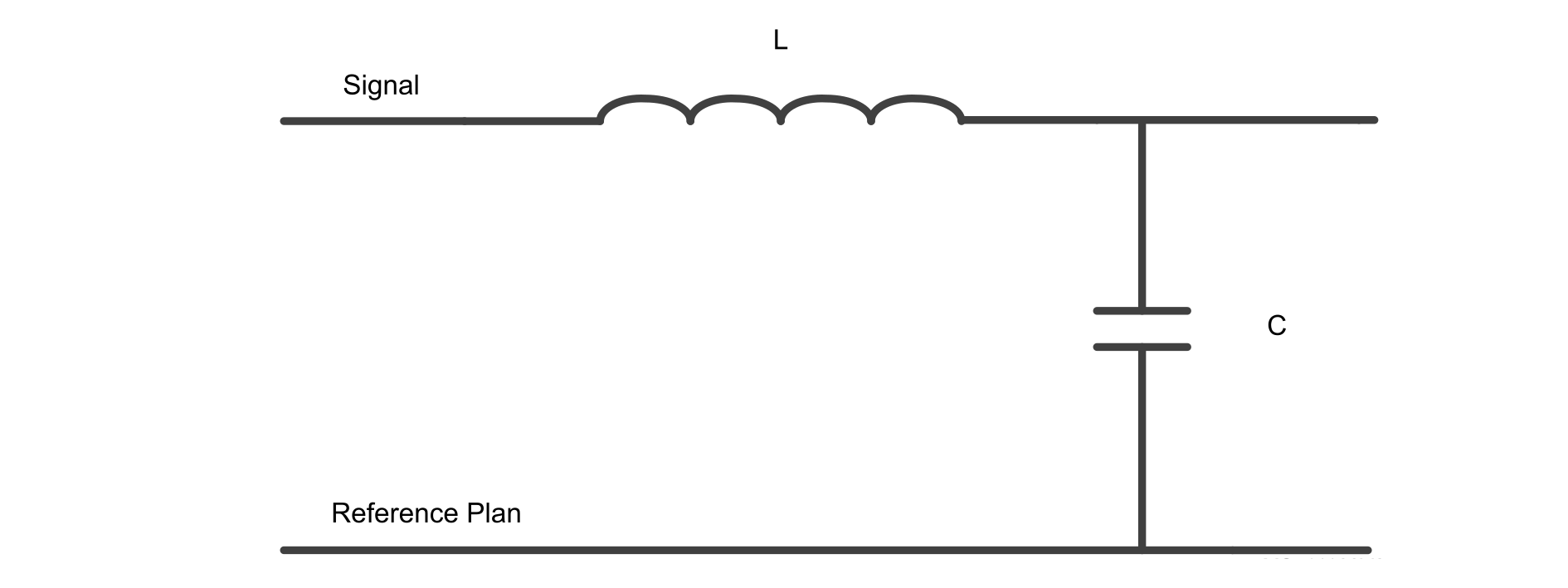
A transmission line is defined as the conductive connection between a driver and a receiver. At low frequencies a wire or a PCB trace is considered to be an ideal circuit (resistive), but at high frequencies, AC (alternated current) circuit characteristics are dominated with inductances and capacitances.
Transmission line model
Figure 1. Transmission line at high frequency
The signals on a transmission line travel at a speed that depends on the surrounding medium. The propagation delay is the inverse of propagation velocity.
1
2
v: propagation velocity, in meters/second
c: speed of light in a vacuum (3 × 10⁸ m/s)
εr: dielectric constant
TD: time delay for a signal to propagate down a transmission line of length x
The propagation delay can also be determined from the equivalent circuit model of the transmission line:
3
Where:
TD: is the time delay for a signal to propagate down a transmission line of length x
L: is the total series inductance for the length of the line
C: is the total shunt capacitance for the length of the line.
The propagation delay is about 3.5 ps/mm in air where the dielectric constant is 1.0. In FR-4 PCBs, the propagation delay is about 7 to 7.5 ps/mm and the dielectric constant is 3.9 to 4.5.
The PCB traces act as transmission lines when the line delay is equal to or greater than 1/6 the rise (or fall) time. The critical length equals 1/6 of the transition electrical length, and the transition electrical length equals to the rise (or fall) times x1/(propagation delay).
For a 2 nanosecond rise time the critical length is 47.6 mm.
Characteristic impedance
The characteristic impedance (Zo) of the transmission line is defined by:
4
Where:
L: is in henries per unit length
C: is in farads per unit length.
At very high frequency or with very lossy lines, the resistive loss become significant.
IBIS model
The IBIS is a behavioral model that describes the electrical characteristics of the digital inputs and outputs of a device through V/I (voltage versus current) and V/T (voltage versus time) data without disclosing any proprietary information.
The IBIS models are used for signal integrity analysis on system boards. These models allow system designers to simulate and therefore foresee fundamental signal integrity concerns in the transmission line that connects different devices.
The potential problems that can be analyzed by means of the simulations include among others:
The degree of energy reflected back to the driver from the wave that reaches the receiver due to mismatched impedance in the line
Crosstalk
Ground and power bounce
Overshoot or undershoot
Line termination analysis
IC modeling
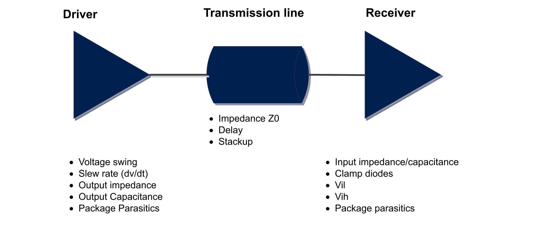
The figure below shows an example of two ICs modeling:Figure 2. Transmission line with IC modeling
Basic structure of an IBIS file
Header
File name, date, version, source, notes, copyright, etc.
Component model data
Default package data (L_pkg, R_pkg, C_pkg)
Complete pin list (pin name, signal name, buffer name, and optional L_pin, R_pin, C_pin)
Differential pin pairs, on-die terminators, buffer selector, etc.
IO model data
All buffer models for the component must be defined in the file
Each flavor of a programmable buffer is separate model
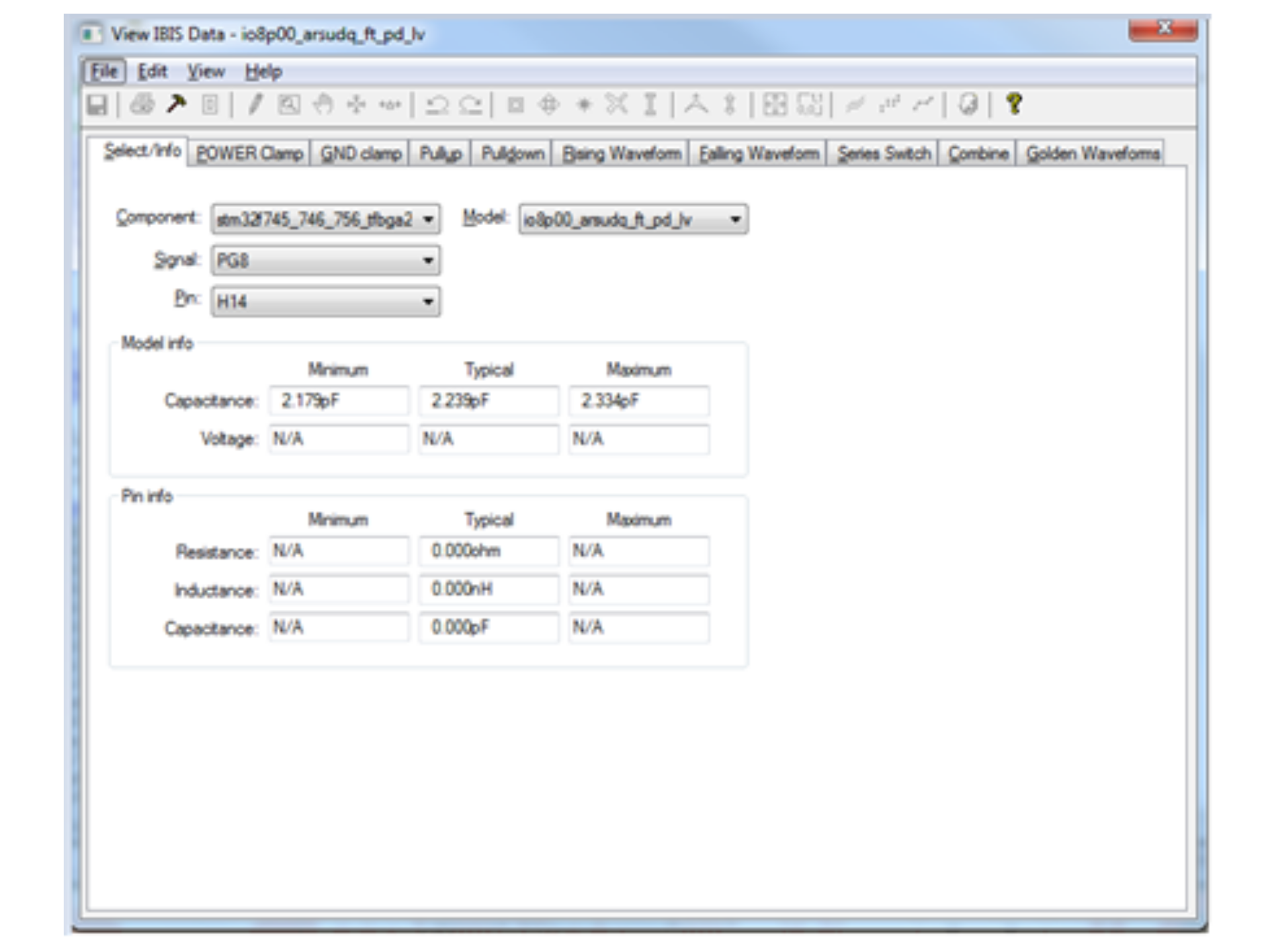
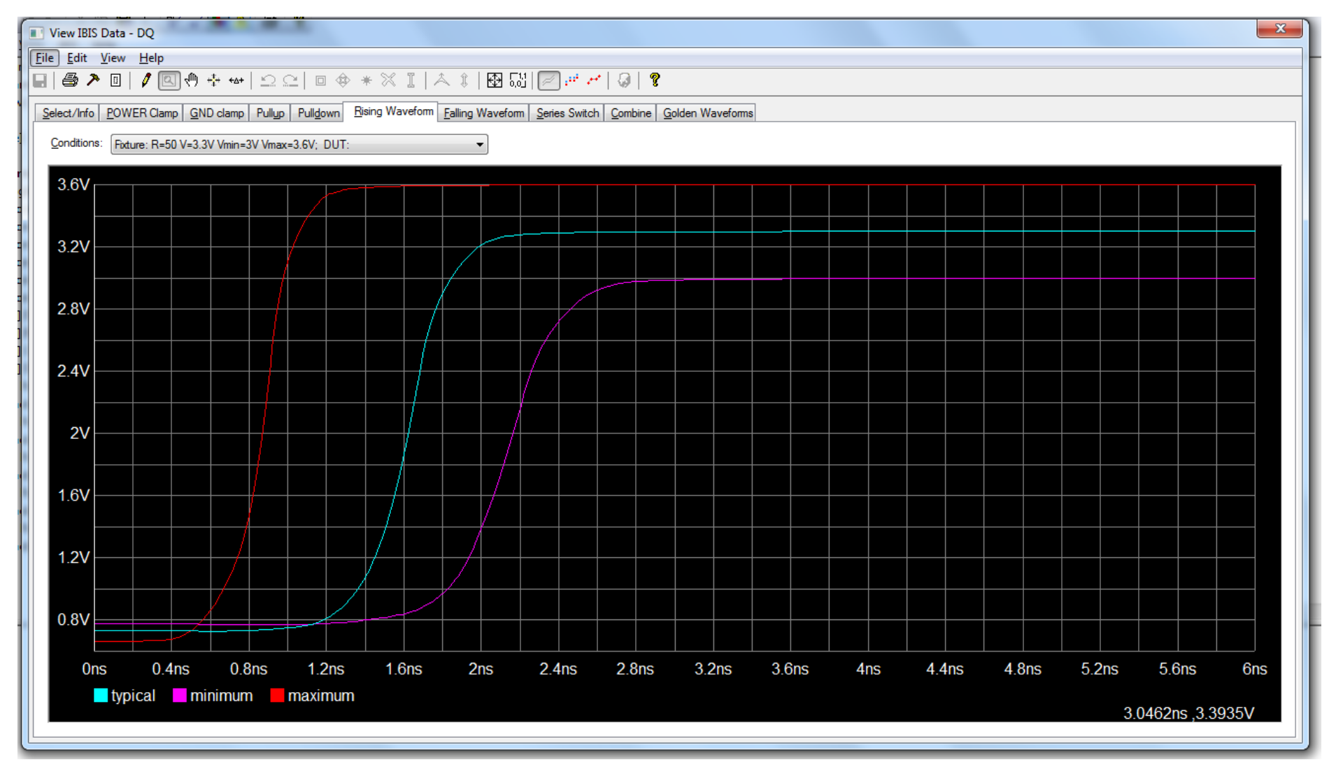
As shown in Figure 3 IBIS editor and Figure 4 IBIS data, the HyperLynx visual IBIS editor is used to open the STM32F746 and the SDRAM (MT48LC4M32B2B5-6A) and to view their characteristics such as the rising and the falling waveforms.Figure 3. IBIS editorFigure 4. IBIS data
STM32 MCUs and MPUs IBIS model selection/selector
This section presents the IBIS model selector of the available GPIO (general-purpose input/output) pin in STM32 MCUs and MPUs.