DDR3L signals
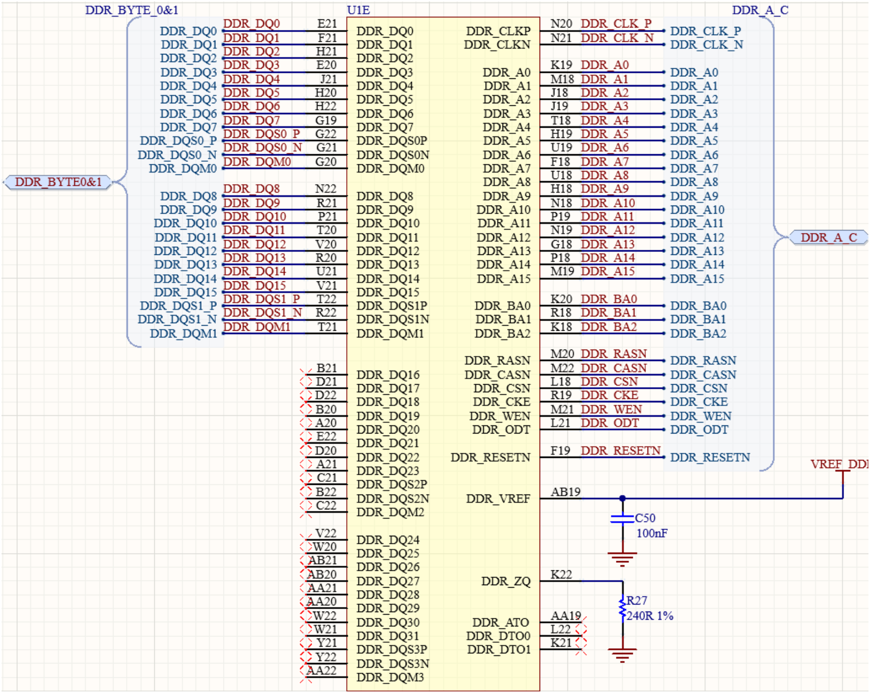
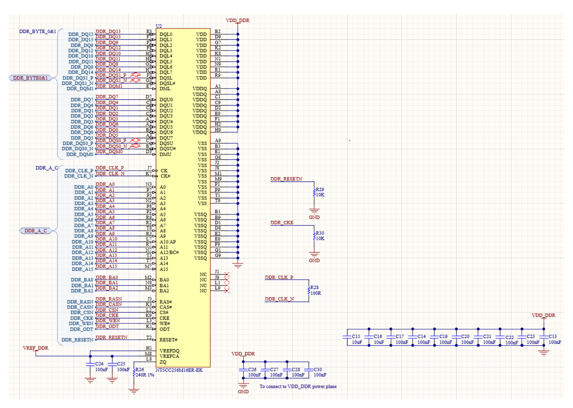
This example shows how to perform a simulation on STM32MP15 Series and DDR3L with DDRx batch simulation of Hyperlynx. The DDR SDRAM has:
- dedicated signals
- differential pair for clock
- address/command, controls
- reference voltage
- calibration resistor
- data lines in which four bytes are each composed with:
- eight data
- a data mask
- differential pair for data strobe
DDR3L simulation
When your layout is finished follow these steps:
- Export your PCB into Hyperlynx file through Altium.
Figure 25. Altium export menu 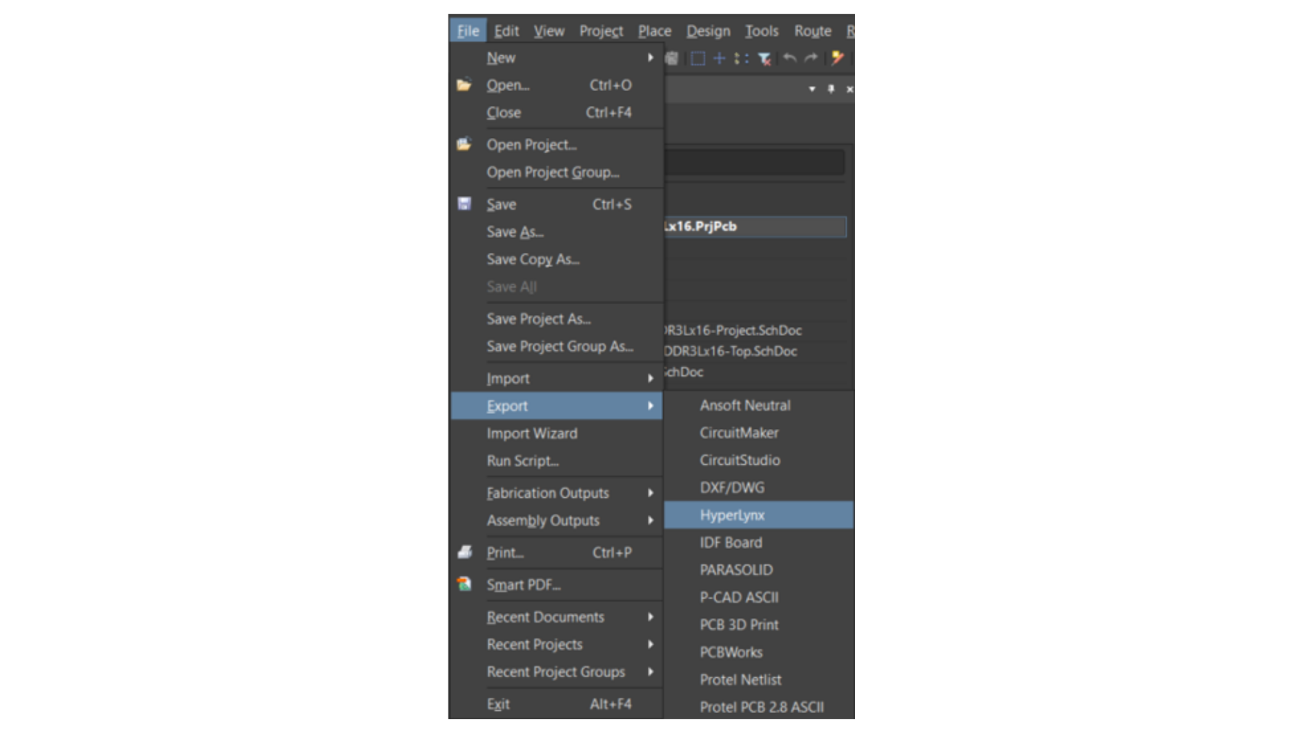
- With Hyperlynx, open .hyp file created.
Figure 26. STM32MP15XXAA PCB 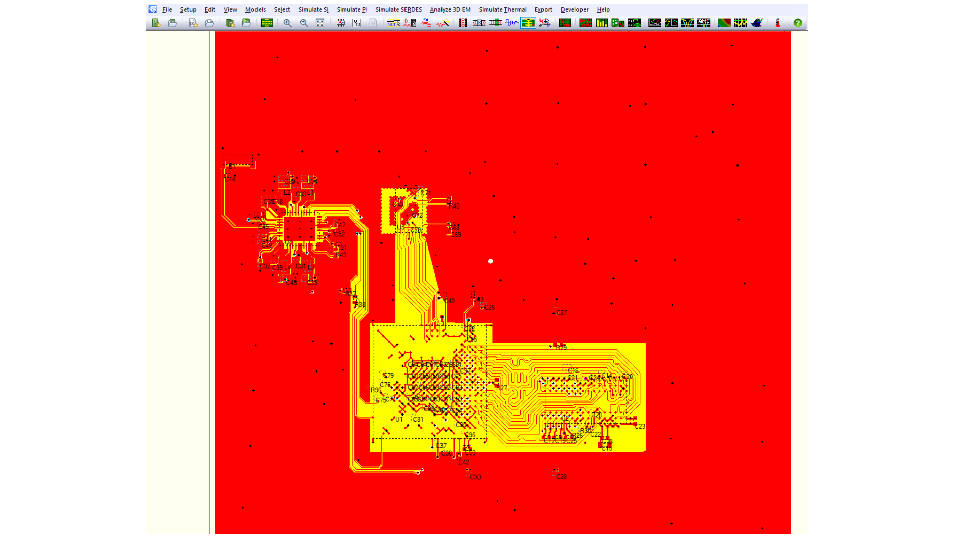
- Assign IBIS model by reference designator.
Figure 27. DDRx batch simulation 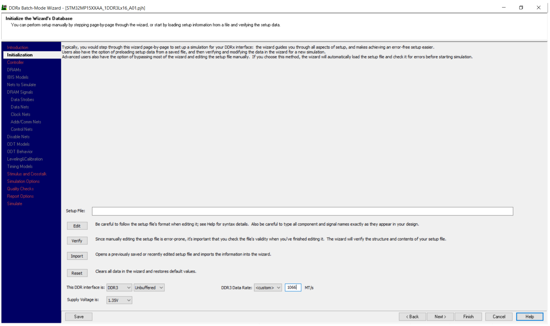
- Select the models of driver impedance and ODT for data, data mask, and differential pair for data strobe
Figure 28. DDRx batch simulation: ODT for data lines 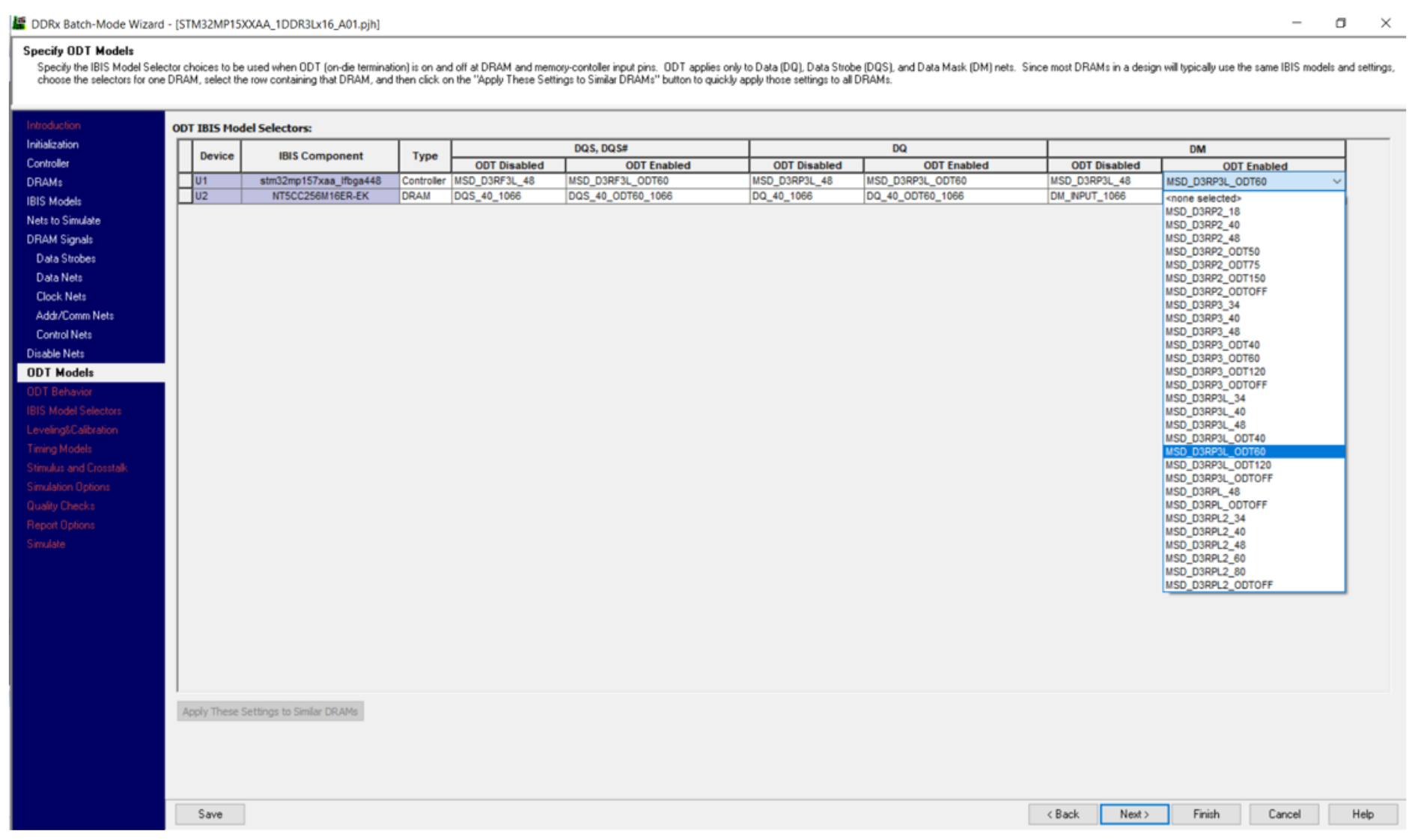 Rule of data naming for output driver impedance in the column ‘ODT Disable’:
MSD_D3RP3_xx for DDR3 single-ended signal, xx is the value of driver impedance
MSD_D3RP3L_ xx for DDR3L single-ended signal, xx is the value of driver impedance
MSD_D3RPL2_ xx for LPDDR2 single-ended signal, xx is the value of driver impedance
MSD_D3RF3_xx for DDR3 differential signal, xx is the value of driver impedance
MSD_D3RF3L_ xx for DDR3L differential signal, xx is the value of driver impedance
MSD_D3RFL2_ xx for LPDDR2 differential signal, xx is the value of driver impedance
Rule of data naming for ODT receiver in the column ‘ODT Enable’:MSD_D3RP3_ODTyy for DDR3 single-ended signal, yy is the value of ODT receiver MSD_D3RP3L_ODTyy for DDR3L single-ended signal, yy is the value of ODT receiver MSD_D3RPL2_ODTyy for LPDDR2 single-ended signal, yy is the value of ODT receiver MSD_D3RF3_ODTyy for DDR3 differential signal, yy is the value of ODT receiver MSD_D3RF3L_ODTyy for DDR3L differential signal, yy is the value of ODT receiver MSD_D3RFL2_ODTyy for LPDDR2 differential signal, yy is the value of ODT receiverFor LPDDR3, use LPDDR2 models. - For the controller, select the models of driver impedance for address/command, controls, and differential pair for clock. Even if clock is a differential signal, for simulation it is set as a single-ended signal. For the DRAM, select the input with the right data rate.
- For the DRAM, select the input with the right data rate.
Figure 29. DDRx batch simulation: non ODT signal 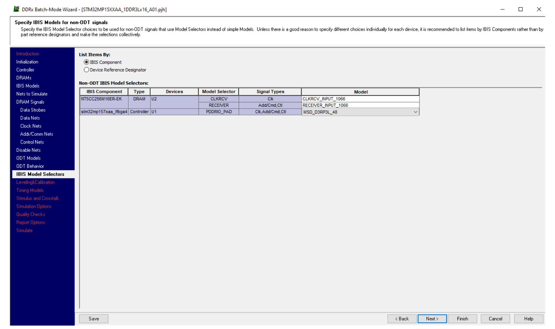 Rule of address/command, control, and clock naming for driver impedance in the column ‘Model’:
MSD_D3RP3_xx for DDR3 single-ended signal, xx is the value of driver impedance
MSD_D3RP3L_ xx for DDR3L single-ended signal, xx is the value of driver impedance
MSD_D3RPL2_ xx for LPDDR2 single-ended signal, xx is the value of driver impedance
For LPDDR3, use LPDDR2 models.Full explanation of model selector can be found in the STM32MP15 IBIS file. - Continue the setup until no issue is detected than click ‘’run Batch Simulation’’.If the simulation is failed, find the best settings in accordance with your design.
Figure 30. DDRx batch simulation: simulate 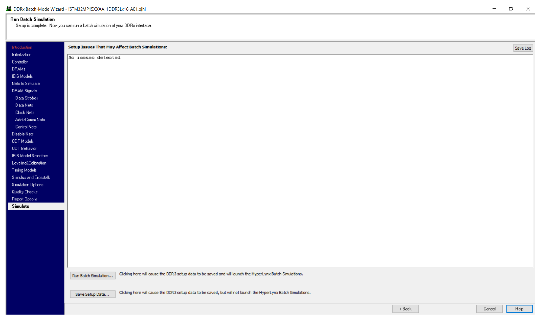
References
- HyperLynx® LineSim User Guide Software Version 9.1, Mentor Graphics, March 2014
- HyperLynx® BoardSim User Guide Software Version 9.2, Mentor Graphics, December 2014
- High-Speed Digital System Design, Hall, Stephen, Hall Garrett, and McCall, James, John Wiley and Sons, Inc., 2000
Revision history
List of tables
List of figures
Figure 1. Transmission line at high frequency
Figure 2. Transmission line with IC modeling
Figure 6. 32F746GDISCOVERY schematic
Figure 7. 32F746GDISCOVERY PCB
Figure 10. Free-form schematic
Figure 11. Waveform with I/O speed of 0x00
Figure 12. Waveform with I/O speed of 0x10
Figure 13. Waveform with I/O speed of 0x11
Figure 14. QUADSPI schematic NOR memory interface
Figure 15. QUADSPI schematic STM32 interface (part 1)
Figure 16. QUADSPI schematic STM32 interface (part 2))
Figure 18. Free-form schematic QSPI_CLK
Figure 19. Waveform with R44 = 0Ω
Figure 20. Waveform with R44 = 33Ω
Figure 21. Terminator Wizard menu
Figure 22. Waveform with R44 = 40.6Ω
Figure 23. DDR3L schematic STM32MP15 interface
Figure 24. DDR3L schematic memory interface
Figure 27. DDRx batch simulation
Figure 28. DDRx batch simulation: ODT for data lines
| Date | Version | Changes |
|---|---|---|
| 1-Avr-2016 | 1 | Initial release. |
| 4-Sep-2019 | 2 | Updated all the document to include MPUs on its scope. |
| 10-Aug-2022 | 3 |
Updated: Added: |