The mathematician Richard Hamming invented the first ECC. The original Hamming code uses 7 bits to store 4 bits of information with redundancy bits used for correction, and detection of errors. In STM32 devices, selected RAM and flash memories are protected using a SEC-DED algorithm based on Hamming principles, but improved with one extra parity bit. The ECC code is capable of detecting and correcting a single-bit error and of detecting a two-bit error in the stored word of data.
In SRAM volatile memory, a stray alpha particle may cause a bit value to flip either way. This is a constant threat and the probability of single-bit failure is the same regardless the age of the hardware. A single-bit or two-bit error failure is a problem especially in applications where large amount of data is stored for long periods of time without reset, for example a battery-powered data logger.
In flash memory, the data decays over time, especially at high temperatures. Storage temperatures have an impact on flash memory data, but cycling (programming) temperature has an even stronger impact. The flash memory can sustain only a certain amount of rewrites to each memory word, this leads to the need of implementation of wear leveling in case of data storage. The typical retention time and life cycle of flash memory for a given product is published in the product datasheet.
Both types of failures (single-bit error and two-bit error), are inevitable, but the correct use of the ECC can prevent data loss.
Table 3. Number of extra check bits used for SEC-DED
Data word width
Number of redundancy bits
16
6
32
7
64
8
128
9
256
10
ECC implications
ECC is a key element in embedded systems that aim to comply with requirements of safety standards such as IEC60730 Class C or IEC 61508 SIL2 and higher.
A system without hardware ECC may still meet target safety standards compliance but it requires a deployment of considerable software overhead. The use of ECC memory to increase the overall diagnostic coverage above 90% is easy to do and increases the system’s readiness to comply with high safety standards. Another advantage of using ECC is the potential improvement of security as ECC usage may lead to detection of hardware tampering.
RAM ECC
The RAM ECC functionality of the STM32 devices has a peripheral-like interface with registers for settings and with interrupts that permit a quick reaction to detected fault. All STM32H72x/H73x/H74x, and STM32H75x SRAM and instruction/data cache memories are protected with ECC. The data width is 64-bit for AXI-SRAM and for ITCM-RAM. All other volatile memories are accessed by 32-bit bus width (word size). On STM32H7Ax/H7Bx, only the tightly coupled memories and instruction/data cache memories are protected with ECC. The other SRAMs are not protected with ECC.
The ECC Monitoring is local per RAM region and each region is controlled by the RAMECC_MxCR. The RAMECC_IER allows a global ECC monitoring of all the RAM sectors when activated whatever the configuration of RAMECC_MxCR
Other series featuring the RAM ECC protection are STM32H5, STM32C5, and STM32U5. Based on Cortex®‑M33, these series have a simpler memory architecture. They have ECC implemented on SRAM regions intended for data, which are backup SRAM, SRAM2, and SRAM3. In case of SRAM3, the use of ECC is limited to the first 256 Kbyte of SRAM3 memory range. Last 64 Kbyte block is then made unavailable for the user, serving for ECC redundancy storage.
Table 4. SRAM ECC coverage in selected STM32 devices
On most of the STM32H7 series microcontrollers, the RAM ECC cannot be turned off (except STM32H7Rx/H7Sx). The ECC is powered and clocked along with the RAM and it is an integral part of the RAM interface. For example, backup SRAM can be disabled. This also disables the RAM ECC controller associated with it.
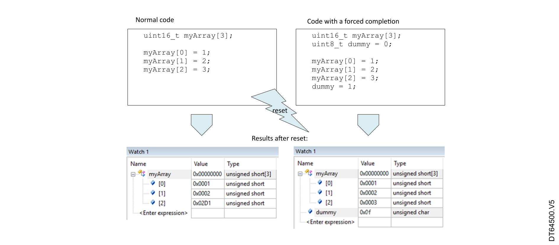
The ECC is computed on data word. If data smaller than a word is written in the volatile memory, the modification is done on a read-modify-write basis. On an incomplete access, the ECC does not write the value immediately. As it may be the very next byte or half word, it waits for the next write access. This is especially important in applications dealing with the backup SRAM. For example when modifying an array of characters, this has a very positive effect on device power consumption. However, a write operation is not completed in case of reset (the memory contents is retained without the last incomplete word write).
The method to make sure the array is always updated entirely is to write a dummy incomplete word write after each regular one. The dummy write address must be within the same memory (backup SRAM in this case).
Figure 1. Unaligned access handling in preserved SRAM
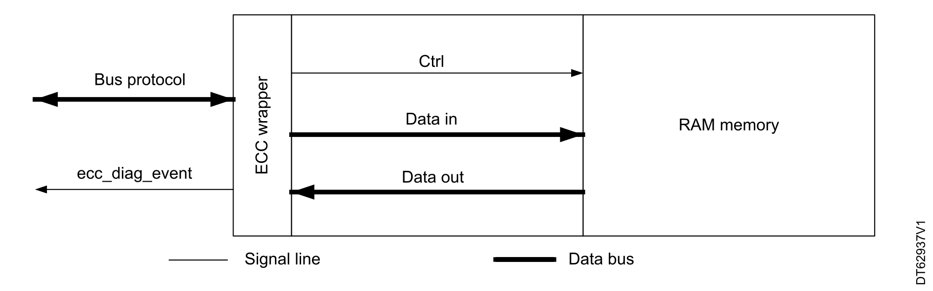
Figure 2. RAM ECC controller interfaced with memory unit
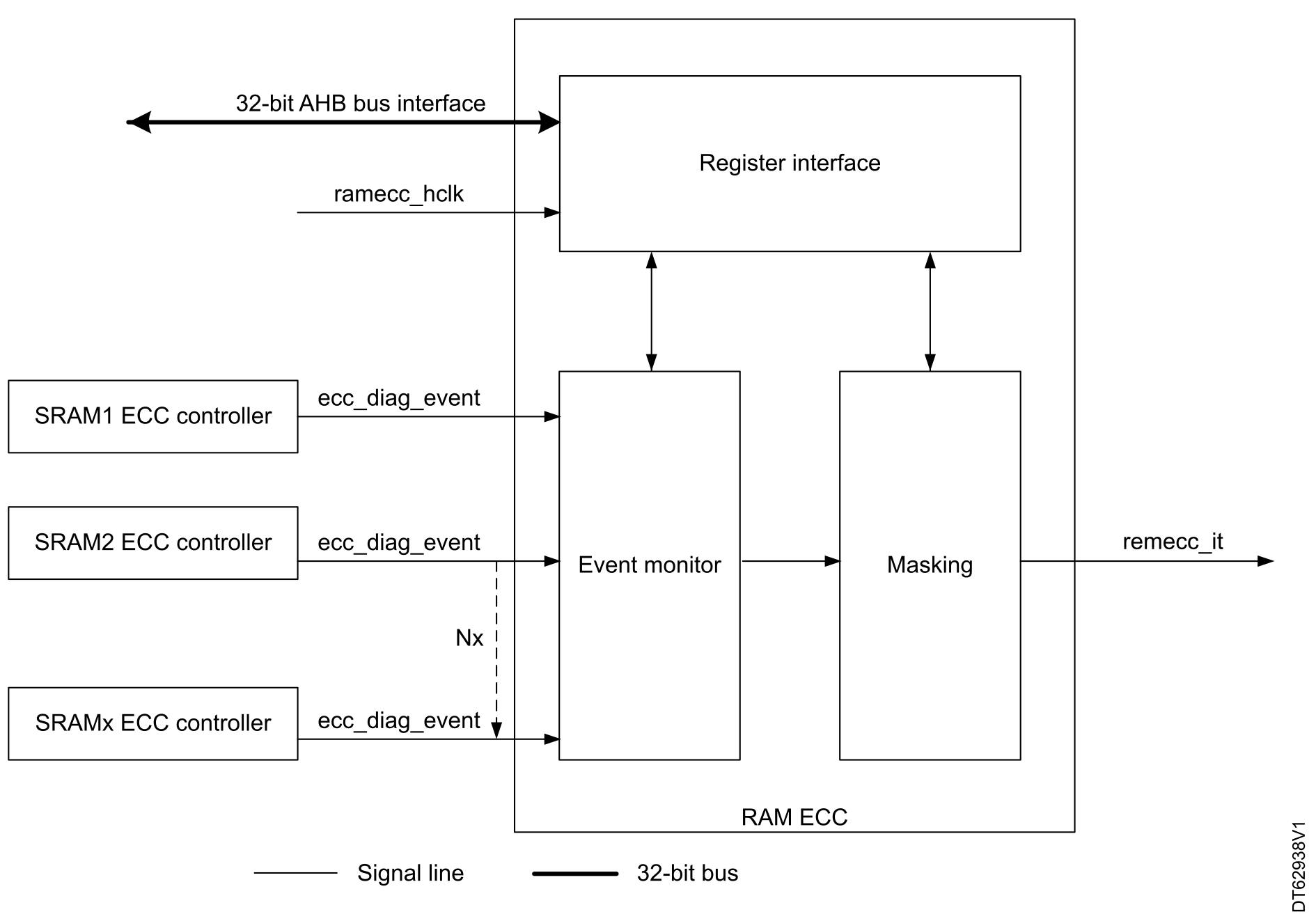
RAM ECC controllers are assigned to each internal SRAM block. Within the STM32H7 architecture, the controllers are usually divided among the three system domains: D1, D2, and D3. Diagnostics from all internal SRAM units/controllers are gathered into a global control block. This global control block has a set of configuration registers and a global interrupt signal with the possibility of event masking.The STM32H7Rx/H7Sx lines are exceptions. They do not share the power domain segmented SRAM. Instead, almost all the SRAM can be accessed on the AXI bus. Parts of SRAM can be relocated between the TCM and AXI mapping. This is the only STM32H7 line where the ECC can be deactivated. This allows the area used for redundancy purposes to be available as the SRAM4.
The STM32U5 series and STM32H5 series microcontrollers have the ECC configurable for each SRAM block individually. Their ECC can also be enabled or disabled by the control bits in the OB space. Direct control of the volatile ECCE (enable) settings in RAMCFG registers is possible, but actually intended for testing rather than use by a fielded application. The STM32C5 series follows the same principle, however the ECC is only available for SRAM2.
Figure 3. ECC RAM simplified block diagram
The particular RAM ECC controller assigned to a specific SRAM block checks the data integrity at each read access to that SRAM block. Some read access types are not obvious, as certain write include an implicit read phase. An example of not-obvious read access is an incomplete RAM write performed as a read/modify/write in two cycles. This can be either write of data smaller than RAM word, or an unaligned write.
1 AXI bus is 64b, but the same memory can also be accessed by AHB.
2 Only the first 256 KB of SRAM3; the last block of memory is used to manage the ECC.