AN5342 · Application noteHow to use error correction code (ECC) management for internal memories protection on STM32 MCUs
Download .pdfOpen in the full document

ECC testing in flash memory

ECC testing in flash memory

For details on dedicated memory methods, refer to the product Reference Manual.

The double write method requires writing sequences of preselected data, matching the length the flash memory word to an empty flash memory address. The memory must not be erased between writes. Reading after the second write triggers the ECC interrupt.

ECC sequences lists sequences that lead to SEC and DED errors for different flash memory word lengths.

The disturbed write method is sensitive to accurate synchronization between the reset and programming operations. It is necessary to execute from SRAM, or at least from a different flash memory bank. Start programming, and then, after a delay of a few microseconds, force a reset. Reading the written address after the reset should trigger the ECC error. It is easy to generate multiple bit errors this way, while consistently reproducing single‑bit errors is difficult. The recommended pattern is to flip a single bit in the written data to 0 and time the reset so that the bit is written and the ECC is not updated.

Some products have the EDATA option, where certain flash memory pages can be reconfigured from code (8‑Kbyte page, 9-bit ECC) to data (6‑Kbyte page, 6-bit ECC). A page reconfigured to 6-bit ECC starts with ECC errors before the first erase because the reconfiguration scrambles the memory contents.

It is possible to keep the memory location programmed with user-created incorrect ECC to reproduce the error as needed. The error is encountered on each read access.
ECC use in applications

In order to correctly use the ECC capabilities, basic routines to deal with detected errors immediately must be implemented in the firmware. It is recommended to log and monitor the error presence for maintenance, failure prediction and hazard warning. This recommendation is especially important for safety and industrial applications.

Dealing with ECC errors in RAM

Static volatile memory is based on a symmetric arrangement of unipolar transistors. The unipolar transistors flip between two states that represent a logical 0 or 1. The amount of energy necessary to make this transition is low, hence the device keeps a low-power consumption.

A stray alpha particle may cause that a bit in the RAM changes its stored value. If the ECC mechanism is not used properly, these rare errors may accumulate over time and cause a data damage or even a system failure.

These events are random by nature and occurrence of error on some address does not provide any indication where or when the next error may occur.

Initialization

When ECC is being used in the RAM, all memories that are to be accessed by the code must be initialized. A read access or an unaligned write to uninitialized memories is likely to trigger the ECC error due to the random initial setting of both the stored value and the redundant bits.

Any pattern is fine for the memory initialization. Find below a proposed list of steps to follow:

  1. Proceed with RAM initialization after POR or after wakeup from Standby mode or after domain standby.
  2. Clear the RAM ECC status register flags after RAM initialization.
  3. Activate the ECC error latching. Even if optional, this action is important for subsequent correction of errors and for reliability errors.
  4. Enable the interrupts for error correction and detection.
    It is possible to selectively enable interrupts only for some memory regions by using register flags for particular RAM ECC controller units.
  5. Enable the global RAM ECC interrupts.

ECC ISR

The interrupt service routine provides an opportunity to immediately react to an event of ECC error. The ISR implemented in CubeHAL generated in projects using STM32CubeMX tool is however just a start. The HAL ISR branches to a callback function. This function is not part of the HAL and this section proposes how it could be implemented..

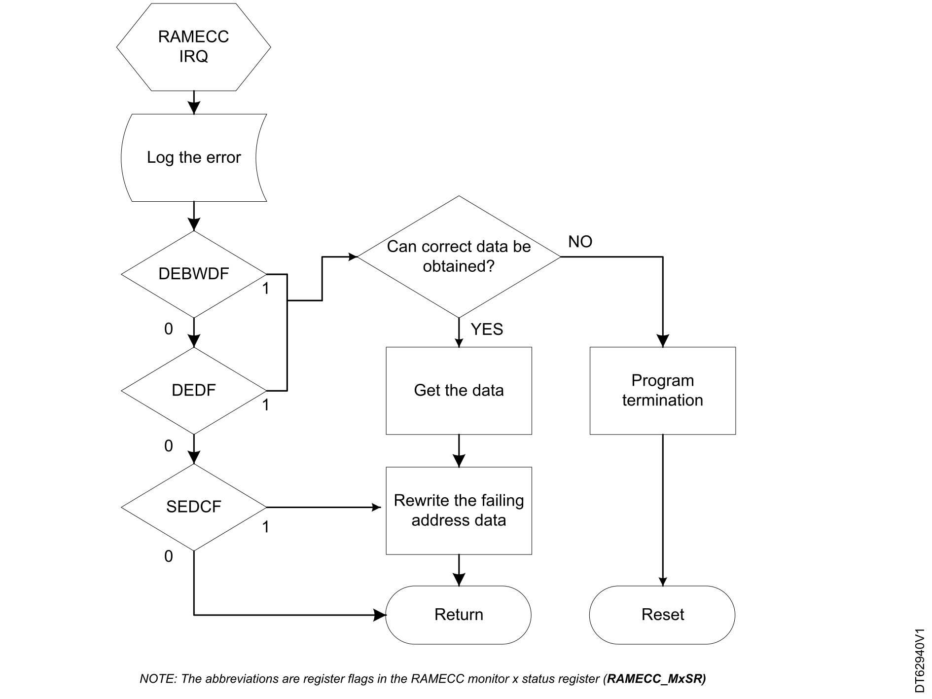
The single-bit errors are automatically corrected by the ECC controller, but only in the data read. It is then necessary to write back the corrected data. In this case, the data and the address latching feature is very helpful. It is appropriate to write the corrected data back to its address. Failing to do so may result in a two-bit failure later (in the case of another bit within the same word is damaged).

If a two-bit error happen anyway, the subsequent action depends on what exactly was damaged. If the affected word is an instruction of code loaded to RAM, the load region within the original code in the flash memory must be identified and the code must be reloaded to the SRAM. The same kind of action is suitable for any other initialized section, for example a copy of the interrupt vector table. As a general rule, in case an instruction cache exists between the SRAM and the CPU, the cache contents must be flushed.

In case of the damaged address falling into a stack area, to avoid further damage caused by executing in incorrect context, a system reset must be performed. If the affected word address lies within boundaries of data RAM (a heap or global variables), it is up to the developer to decide which action to take. Generally a reset is recommended, but risk analysis conclusion may differ case by case.

Figure 4. RAM ECC interrupt actions example

Logging the error for subsequent analysis can be an optional part of the post-failure operation.

Interpreting FAR (failing address register)

The FAR (failing address register) is not showing the absolute address of the failure, but a relative location. The value in FADD[31:0] also points a word and not a byte. To compute the physical address of the failure use the following formula:

Address = Memory start address + FADD x word size in byte

For example, AXI SRAM monitor FADD=0x2004 means 0x2400 0000 + 0x2004 x 8 = 0x2401 0020 (64-bit words) But in SRAM1 monitor the FADD=0x2004 value interprets as 0x3000 0000 + 0x2004 x 4 = 0x3000 8010 (32-bit words).

A special case is DTCM and other memories, which are interleaved. To be specific, it works as follows with STM32H7 series:

  • D0TCM starts at 0x20000000

  • D1TCM starts at 0x20000004

In D0TCM, the address = D0TCM start address + FADD x 8 and in D1TCM address = D1TCM start address + FADD x 8. Each 64 bit of the DTCM consists of 32 bits from D0TCM followed by 32 bit of D1TCM forming common address space, but with separate ECC reporting.

Preventive actions for ECC in RAM

The RAM ECC events are random, hence some damage can be prevented by performing a periodic check on the used RAM area. The ECC check is activated by reading from each word; if the checkup period is appropriate, most erroneous words are detected while there is still only one wrong bit. An appropriate period can vary from hours to several days, it depends on the operating conditions, and the role of the microcontroller.

A preventive ECC checkup does not need to be completed in a single round. It is a background task that may be performed during idle moments, either by a background process or by a low-priority DMA transfers. A single loop or a DMA transfer is not possible as the SRAM is divided into non continuous address ranges.

In the case of the STM32H7 series, the MDMA is particularly suited for this task, as it can access the ITCM/DTCM. When using the Cortex®-M7 CPU for memory check-by-read, the cache is involved (if cache is enabled). Accessing the SRAM through the Cortex®-M7 cache (so ITCM and DTCM are excluded from this rule), each read from memory fills the cache line of 256 bits. The loop that activates the ECC check on each memory word read only the first word of each 256-bit and the cache line loading continues with the remaining words. This action lowers the CPU load, but the bus remains heavily loaded.

Regular GPDMA is adequate for sweeping the memory of the STM32H5 and STM32U5 series.

Note:

It is useful to track ECC incidents in memory. The monitor configuration registers in certain STM32H7 series products allow activation of failure counters.

Dealing with ECC errors in flash memory

Typical failures for the flash memory are fail due to memory cell wear and fail due to charge leakage. Some factors that might contribute to failure are interference from adjacent cell or voltage instability during programming. Unlike to SRAM, failure in certain flash memory address may indicate a slightly higher probability of a subsequent failure in the same page. Flash memory errors should be non-existent on a new device, with probability of failure increasing towards the end of projected lifetime. The flash memory lifetime depends mainly on temperature conditions and the amount of erase cycles.

Flash memory ECC ISR

For the flash memory of the STM32H7 series, the interrupts that notify of an ECC error are included in the flash memory global interrupt vector. The ISR checks the flash memory status register FLASH_SR1 for ECC flags “single error correction” and “double error detection” and take the appropriate action (which depends on the flash memory use). In case of ECCD, it is necessary to flush instruction cache and prevent passing corrupted opcode to the CPU. This task requires special attention, as the BusError is signaled on ECCD. Given that the interrupt vector is shared with normal flash memory operations (such as end of programming), the ISR should then pass control to HAL to deal with the other flags. On the STM32H5 series, STM32U5 series, and STM32C5 series, the ECCC is signaled using a regular flash interrupt vector, while the ECCD issues a nonmaskable interrupt.

Flash memory code

The on-chip nonvolatile memory is primarily intended to be used for code. The code is not likely to be frequently rewritten, so if a damage occurs it is most likely caused by aging and by charge leakage. On a dual-bank device it is possible to have a second copy of the same code and swap to this second copy when an ECC error is indicated. This solution implies that the health of both bank contents is monitored. It is possible to reprogram the failing contents of the other bank from the healthy bank, however there is no guarantee on how much this action might improve the device life expectancy.

EEPROM emulation

If the failing Flash memory cell is used to store data, the failure cause is likely to be linked to a program/erase cycling. Advanced EEPROM emulation implementations include mechanisms that deals with failing memory cells and are able to exclude them from the cycling. The application note EEPROM emulation techniques and software for STM32 microcontrollers(AN4894) deals with the problematic of EEPROM emulation including the ECC implications.

Preventive action for ECC in flash memory

The CRC hardware module of the STM32H7 series is a useful tool to monitor the embedded flash memory health. CRC can check either the whole bank or a specific address range autonomously; ECC is implicitly checked on read as well. The program must then implement a reaction to a detected problem.

For products without this CRC feature, DMA, for example, may be used to check on rarely used portions of code. If the secure boot is in place, such periodical checkups of installed applications and loader code can be implemented here.