AN4312 · Application noteHow to design surface sensors for touch sensing applications on STM32 MCUs
Download .pdfOpen in the full document

Charge transfer acquisition principle

Charge transfer acquisition principle

The surface charge transfer acquisition is a proven, robust and efficient way to measure a capacitance. It uses a minimum number of external components to operate with a single ended electrode type. This acquisition is designed around an analog I/O group that is composed of four GPIOs. Several analog I/O groups are available to allow the acquisition of several capacitive sensing channels simultaneously and to support a larger number of capacitive sensing channels. Within a same analog I/O group, the acquisition of the capacitive sensing channels is sequential.

One of the GPIOs is dedicated to the sampling capacitor (CS). Only one sampling capacitor I/O per analog I/O group must be enabled at a time.

The remaining GPIOs are dedicated to the electrodes and are commonly called channels. For some specific needs (such as proximity detection), it is possible to simultaneously enable more than one channel per analog I/O group.

The surface charge transfer acquisition principle consists of charging an electrode capacitance (CX) and transferring a part of the accumulated charge into a sampling capacitor (CS). This sequence is repeated until the voltage across CS reaches a given threshold (VIH in our case). The number of charge transfers required to reach the threshold is a direct representation of the size of the electrode capacitance. When the electrode is “touched”, the charge stored on the electrode is higher and the number of cycles needed to charge the sampling capacitor decreases.
Surface capacitance

A capacitance is modified when a finger gets close to a sensing electrode. The return path goes through one of the following paths:
  • a capacitor through the user's feet
  • a capacitor between the user’s hand and the device
  • a capacitor between the user’s body and the application board through the air (like an antenna)
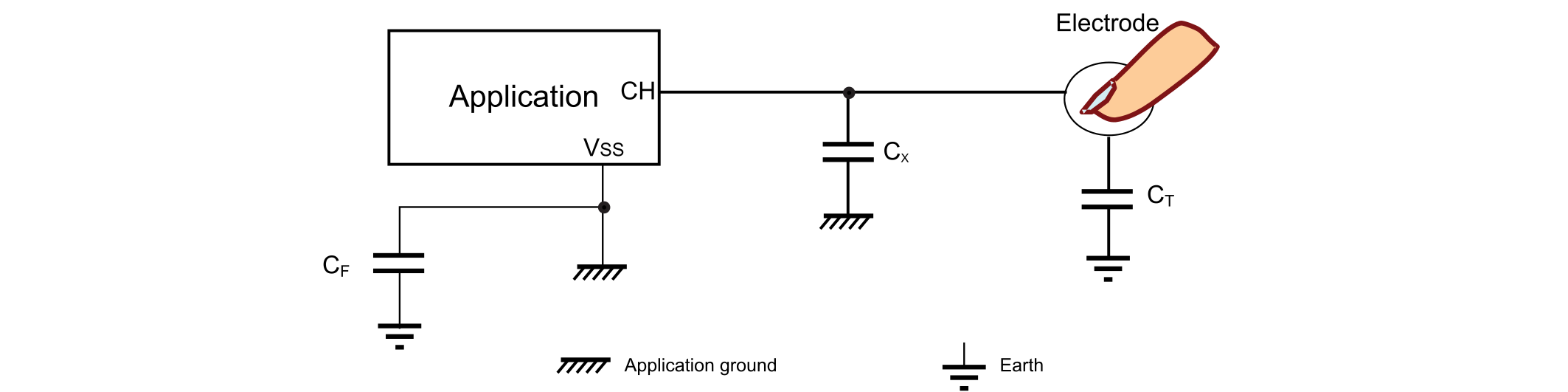
The figure below gives an overview of a system equivalent capacitances location.
Figure 1. Equivalent touch sensing capacitances


where the capacitances are the following:
  • CX is the parasitic capacitance of the electrode.
  • CX is composed of the two following capacitances:
    • The first one refers to earth, is not significant, and can be ignored.
    • The second one refers to the application ground and is dependent on the PCB or the board layout.

      This latter parasitic capacitance includes the GPIO pad capacitance and the coupling between the electrode tracks and the application ground. The PCB and board layout must be designed to minimize this parasitic capacitance.

  • CF is the feedback capacitance between earth and the application. Its influence is important in surface capacitance touch sensing applications, especially for applications that do not feature a direct connection to earth.
  • CT is the capacitance created by a finger touch. This capacitance is the source of the useful signal. Its reference is earth and not the application ground.

The total capacitance measured is a combination of CX, CF and CT, where only CT is meaningful for the application. The total capacitance is given by the following formula:

C x + 1 1 C T + 1 C F

Overview

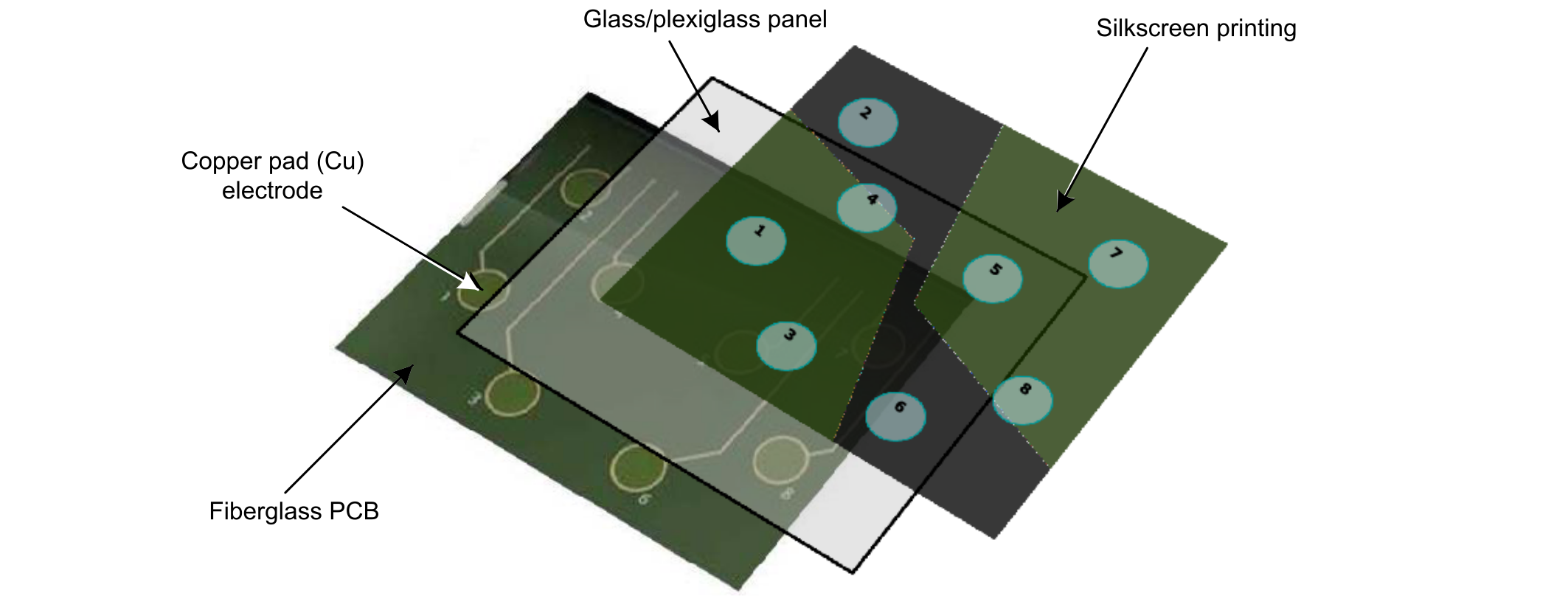
A surface capacitive sensor is generally made up of the following different layers (see the figure below):
  • a fiberglass PCB
  • a set of electrodes made of a copper pad
  • a panel made of glass, Plexiglas, or any non-conductive material
  • a silk screen printing
Figure 2. Example of capacitive sensor construction

Substrates

The substrate is the base material carrying the electrodes. A substrate can be chosen among any non-conductive material: in practice, PCB materials (such as FR4 or CEM-1), acrylics like polyethylene terephthalate (PET) or polycarbonate. Glass is also an excellent material for this purpose.

In many cases, the substrate used in electronic application works also well for capacitive sensing. Special care is required to avoid materials that can retain water contained in the atmosphere (e.g. hygroscopic material such as paper based). Unfortunately, this modifies εR (relative permittivity) with environmental conditions.

It is not recommended to directly set the substrate against the front panel without gluing it by pressure or by bonding. Some moisture or air bubbles may appear between them and cause a change on the sensitivity. Closely link the substrate and the panel together avoids a varying sensitivity loss that is hard to predict (when the air bubbles are greater than 2 mm diameter).

The substrate and the panel can be strongly glue mechanically or with a suitable bonding material.

It is also possible to construct sensors that do not rely on a substrate (refer to Transfer of an electrode from PCB to the front panel, Using electrodes separated from the PCB and PCB and layout).

Electrode and interconnection materials

Generally, an electrode is made with the following materials: copper, carbon, silver ink, Orgacon™ or ITO (indium tin oxide).

The resistance to electric current of a material is measured in ohm-meters (Ωm). The lower this degree of resistivity the better, as well as a good RC time constant. That is why interconnections are made with low Ωm material. A printed silver track at 15.9 nΩm that is 100 mm long, 0.5 mm wide and 0.1 mm thick (so the area is 0.05 mm²) has a resistance of 32 µΩ.

About metal deposition, another well-known approach is to consider the Ω/□ (pronounced “Ohms per square” and called sheet resistance. Knowing this constant (given by the manufacturer) and how many squares are put in series, allows the evaluation of the overall resistance of the line).

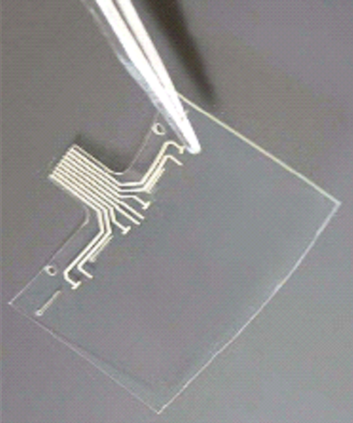
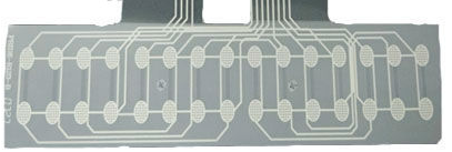
For instance, silver and ITO (about 10 times greater) can be compared and the material well suited for the connections can be then identified (see the figures below).
Figure 3. Clear ITO on PET with silver connections
Figure 4. Silver printing on PET

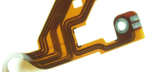
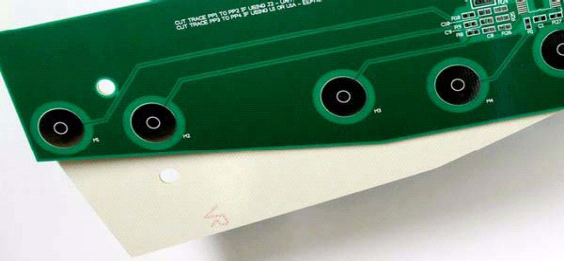
More and more applications need a flex PCB or FFC/FPC (flat flexible conductor/flexible printed circuit (see Figure 5 Flexible PCB (FPC) and Figure 6 FR4 (2-sided epoxy-fiberglass)) to interconnect circuitry. It is suitable if the overall application is mechanically stable. Furthermore, the FPC tracks are part of the touch sensor. If the flex moves a little bit, even a few micrometers, the capacitance to its surroundings definitely changes and may be significant, causing false touch detections or drops in sensitivity. Putting the flex in close proximity to a metal chassis or other signals, or on top of noisy circuitry, can cause problems as well (loss of sensitivity or spurious detection).

Table 2. Potential application problems with flex PCB placement
When the flex PCB is in close proximity to......the following can occur.
...the ground or to a metal chassis connected to the ground....the sensitivity is reduced.
... a floating metal object or to a floating metal chassis... the object or the chassis conducts the touch to the electrode.
... a source of noise... the acquisition is strongly perturbed and so the touchkey becomes non-usable.
Figure 5. Flexible PCB (FPC)
Figure 6. FR4 (2-sided epoxy-fiberglass)

Panel materials

The panel material can be selected to suit the application. This panel material must not be conductive. The material characteristics impact the sensor performance, particularly the sensitivity.

Dielectric constant

The panel is the main item of the capacitor dielectric between the finger and the electrode. Its dielectric constant (εR) differentiates a material when placed in an electric field. The propagation of the electric field inside the material is given by this parameter. The higher the dielectric constant, the better the propagation.

Glass has a higher εR than most plastics (see the table below). Higher numbers mean that the fields propagate through more effectively. A 5 mm panel with an εR of height performs similarly in sensitivity to a 2.5 mm panel with a relative epsilon of four (all other factors being equal).

A plastic panel up to 2 mm thick can be used, depending on touchkey spacing and size. The circuit sensitivity must be adjusted during development to compensate for panel thickness, dielectric constant and electrode size.

The thicker a given material is, the worse the SNR. For this reason, it is always better to try and reduce the thickness of the front panel material. Materials with high relative dielectric constants are also preferable for front panels as they help to increase SNR.

Table 3. Dielectric constants of common materials used in a panel construction
Material εR
Air 1.00059
Glass 4 to 10
Sapphire glass 9 to 11
Mica 4 to 8
Nylon 3
Plexiglass 3.4
Polyethylene 2.2
Polystyrene 2.56
Polyethylene terephthalate (PET) 3.7
FR4 (fiberglass + epoxy) 4.2
PMMA (Poly methyl methacrylate) 2.6 to 4
Typical PSA 2.0 - 3.0 (approx.)

Sensitivity

A useful parameter to consider with panel material and thickness (T) is the electric field equivalent vacuum thickness TV, given by the following formula:

TV = t ϵ R

where t is the thickness of the dielectric.

TV is the thickness of vacuum with an electric field conduction equivalent to that of the material. The smaller it is, the easier the field can reach through. Panels with the same TV make touchkeys with identical sensitivity. This works for both directions and may be used to evaluate the touch sensitivity from the back side of the application.

For a panel built from a stack of different materials, it is possible to add the vacuum equivalent thickness of each layer as shown in the following formula:

TV(STACK) = ∑   T V ( l a y e r s )

Each material has an influence on the sensitivity. The equation can be used when, for example, the electrodes are on the bottom surface of the PCB substrate, then the thickness and εR of the substrate are factors of the global sensitivity.

Mechanical construction and PCB to panel bonding

In order to ensure stable touch detection, the PCB must always be at the same place on the panel. The slightest variation, even as small as 100 μm, may lead to differences in the signal that can be detected. This must be avoided to ensure the integrity of the touch detection.

The panel and other elements of the device must not be moved, or only as little as possible, by the user’s finger. To avoid this kind of problem, glue, compression, co-convex surfaces can be used to mechanically stabilize the PCB and the panel very close together (using for example heat staking plastic posts, screws, ultrasonic welding, spring clips or non-conductive foam rubber pressing from behind).

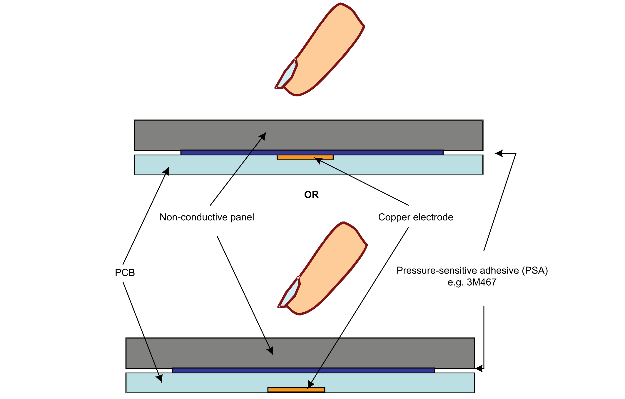
Normal construction is to glue a sensor to a front panel with pressure sensitive adhesive (PSA). 3M467 or 468 PSAs work very well.
Figure 7. Typical panel stack-up

Metal chassis

A metal chassis behind a touch sensor is a good path to the ground and tends to reduce the sensitivity of the touch response in case there is a significant area of overlap. Such a metallic surface must never be electrically floating as it makes the whole product unstable in terms of touch detection. This is also applicable for any conductive decorative feature close to the sensor.

Metal chassis and decorative items must be grounded or connected to the driven shield (see Driven shield) if it is implemented.

Metallic paints can be an issue if they contain conductive particles. Low particle density paint is recommended.

Air gap

Due to its dielectric constant, air can be used as an isolator. An air gap reduces the touch sensitivity when it is in the touch side stack. However, in some conditions, air can be useful to reduce the ground loading in the non-touch side stack. Such ground loading can be due to the metal chassis or an LCD. For instance, when designing a touch-screen solution, an air gap of 0.5 mm to 1 mm between the LCD and the touch sensor is recommended. Air gaps also help to reduce the sensitivity of the back side of a portable device.