Power dissipation and cooling methods
- power dissipation and its variation with factors named PVTA (process, voltage, (junction) temperature, and activity)
- how to minimize the power consumption
- how to optimize the thermal dissipation
The static/leakage current grows exponentially with the junction temperature (while the dynamic current does not significantly change).
Therefore, the total current can be written as follows:
The dissipated power varies with PVTA conditions. It is calculated as the product of the voltage generated across the device and the (average) current consumed.
The junction temperature increase above the ambient temperature is calculated as a product of the dissipated power and the junction-to-room thermal resistance.
The junction temperature must be kept lower than the maximum target given by the following equation:
In this simplified formula used only for didactic purpose, Theta_j_room is a complex coefficient that is not a device characteristic but a system one (device + other components + boards + casing).
To reduce the power consumption, the first action is to reduce the supply voltage. Some STM32 devices offer a multipower domain architecture that allows the different power domains to be set in low-power mode. The goal is to optimize the power efficiency (see the corresponding datasheets for more details).
The power consumption profile also varies with the application. Some applications are most of the time in idle mode, working on full or limited capacity only when an event occurs. Some others demand a regular workload.
For these various power profiles, the user programmer enables the low-power modes by software.
All these modes are available, for example, on STM32H7 and STM32MP1 series devices (see the reference manuals for more details).
In this section, process, voltage, and activity factors are kept constant, and there is a focus on the effect of the junction temperature.
The static/leakage current grows exponentially with the junction temperature (while the dynamic current does not significantly change).
When performing system-level thermal simulations in the design phase, it is fundamental to input junction temperature dependent power dissipation.
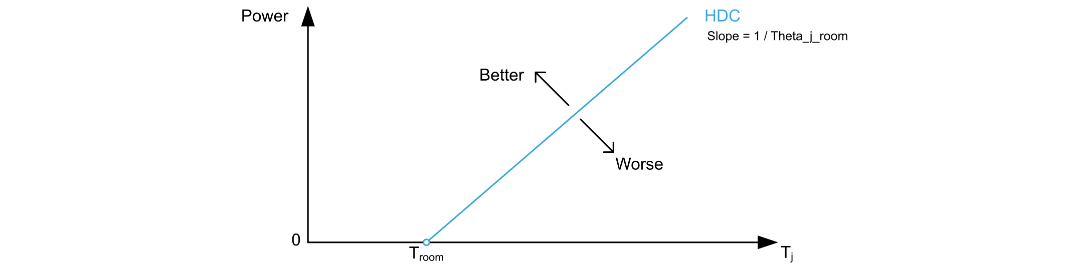
The junction-to-room temperature thermal resistance, Theta_j_room, characterizes the cooling system of a design.
This thermal resistance gives the capability to dissipate power in the design while limiting the junction temperature.
The following equation gives the heat dissipation capability (HDC):
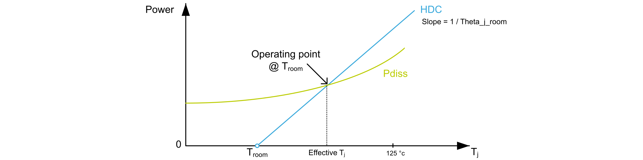
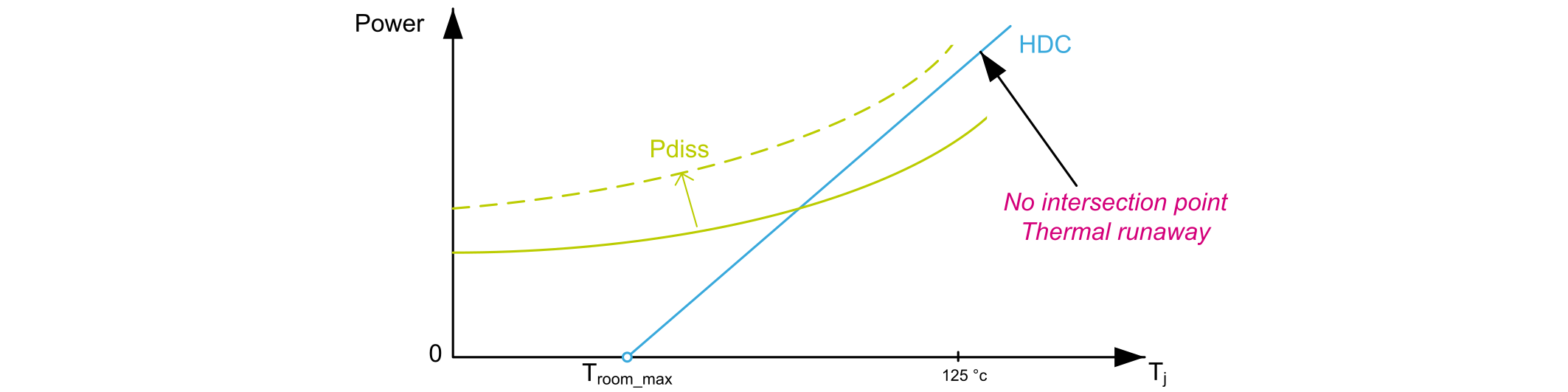
The figure below shows the operating point at the intersection of the curve of the power that can be dissipated inside the design at a given TJ (HDC) and the curve of the power effectively dissipated inside the design (Pdiss).
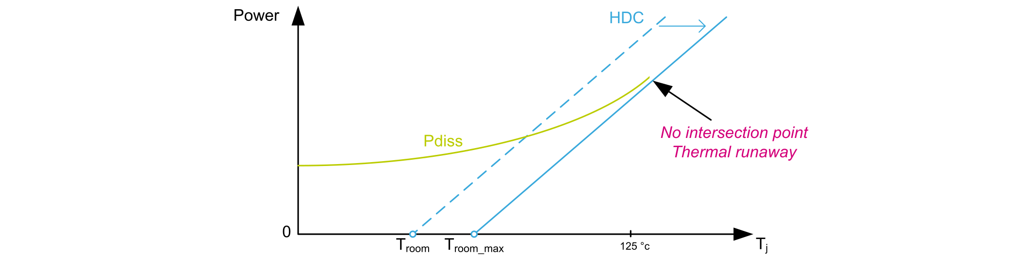
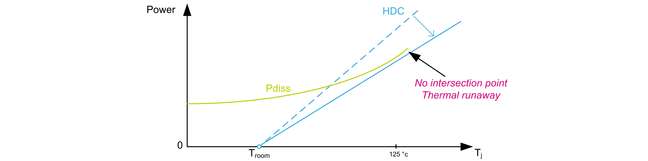
The cooling design is safe (no thermal runaway) if an intersection point exists for Troom = Troom_max, with a junction temperature < 125 °C.
The two curves in case 2 and case 3 do not intersect. For this reason, no stable operating point is defined. This is a condition of thermal runaway.

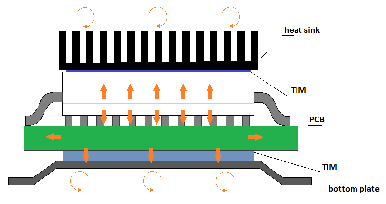
The heat sink and the PCB dissipate the power to the surrounding environment by the convection and radiation methods.
The term ‘natural convection’ is used when no fan is used in the casing. This cooling method is a combination of natural convection and radiation that always work in parallel.
The term ‘forced convection’ is used when a fan is used in the casing.
| Comparison factors | Natural convection | Forced convection |
|---|---|---|
| Cooling efficiency | Low |
Medium to high (depending on air speed) |
| Cost | Low (no fan) | Higher (cost of the fan) |
| Reliability |
Higher (no moving parts) |
Lower (mechanical part moving) |
| Acoustic noise | None |
Small to medium (depending on air speed) |
| Possibility to control cooling efficiency based on needs | None | Yes, by varying fan voltage |