Bottom cooling - host PCB design
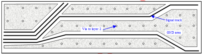
To provide enough ‘thermal vias’, as the host PCB is a secondary heat sink for the device, it is important to use the recommended stack-up and to optimize the PCB layout beneath the package.
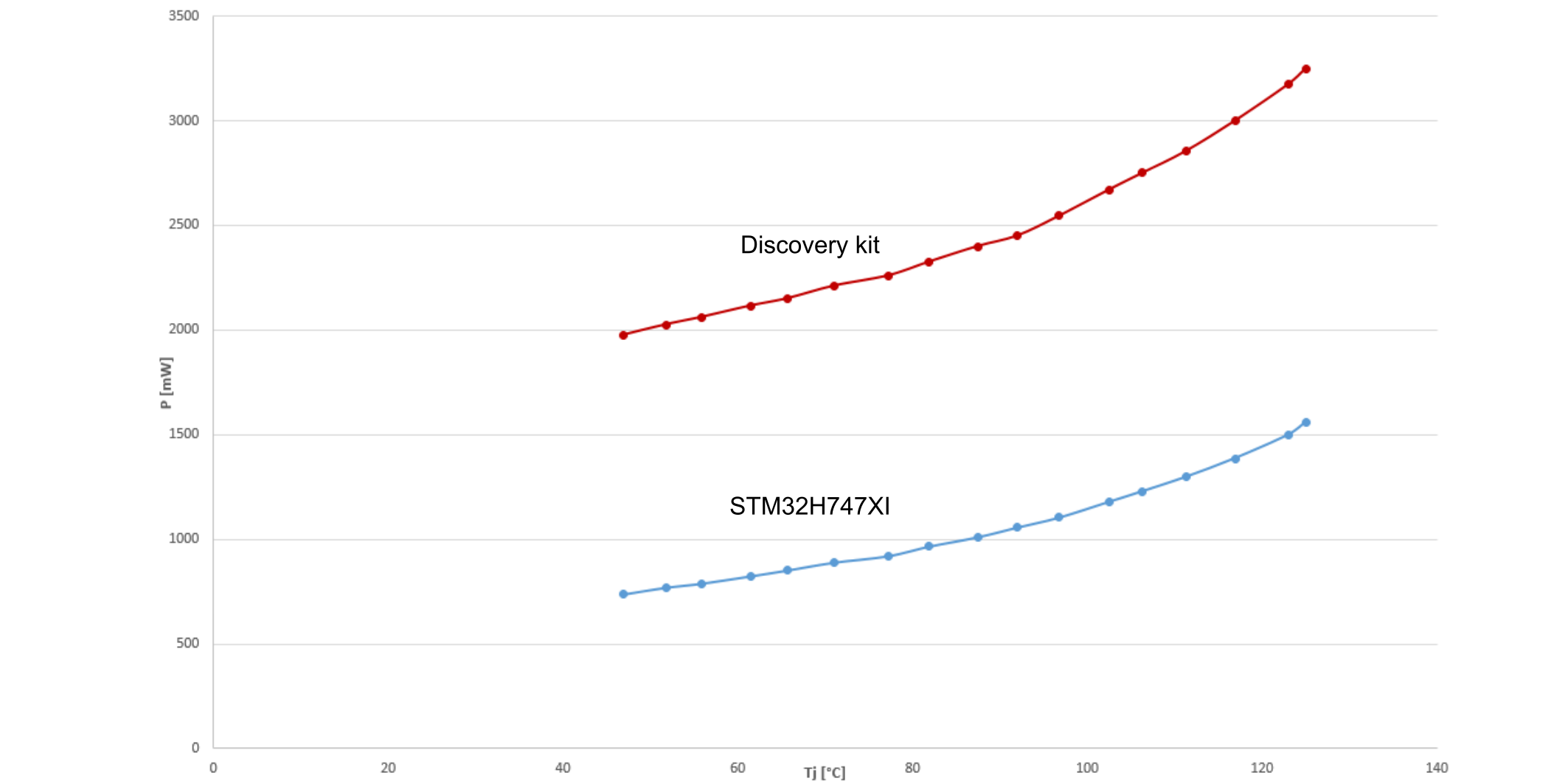
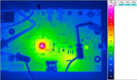
A significant power proportion is drawn from the package to ambient air through the host board by the paths detailed in the next sections (sorted by decreasing order of importance). The design rule implementation for ground and power connections is necessary for cooling and power distribution.
It is not possible to produce a set of rigid rules for layer construction within a PCB because each design has its own requirements.