AN5036 · Application noteGuidelines for thermal management on STM32 MCUs and MPUs
Download .pdfOpen in the full document

STM32 thermal parameters

STM32 thermal parameters

Most of the STM32 datasheets give only Theta‑JA thermal resistance, but some specify also Theta‑JC and Theta‑JB, defined in the table below.
Table 2. STM32 thermal resistances
Thermal metric Symbol Value Main purpose
Theta‑JA θJA
T J − T A P T O T
Used to rank package performance in the JEDEC environment
Theta‑JC θJC
T J − T C P C

Used to rank package performance

Used in simulations with a 2R model (2R = two resistances)
Theta‑JB θJB
T J − T B P B

Used to rank package performance

Used in simulations with 2R model
These parameters are determined under the following specific conditions that differ from the final application conditions:
  • Theta‑JA: The JEDEC51-2 document Integrated circuits thermal test method environmental conditions - natural convection (still air) describes the thermal test method to define Theta‑JA.
  • Theta‑JB: The JEDEC51 document Integrated circuit thermal test method environmental conditions – junction-to-board describes the thermal test method to define Theta‑JB.
  • Theta‑JC: The MIL‑STD-883E document Test method standard microcircuits describes the thermal test method to define Theta‑JC.

These thermal resistances must be carefully defined in semiconductor packages and devices context.

The most important point about these values is that the total power dissipated by the device flows between the two following “points”:
  • The junction
  • Ambient or board temperature

There are no extraneous parallel thermal paths in the system allowing some of the heat to “leak” away. All the heat leaving the junction eventually arrives at or passes through the other point.

It is usually possible to know the total power dissipation of a device but it is far more difficult to know which fraction of the heat flows out through the case top, versus the part that flows through the leads, and versus the part that flows through the air gap under the package.

Theta‑JC and Theta‑JB are generally used as inputs for thermal simulation tools, which calculate which fraction of the heat flows out through the top and the bottom of the device.
Power dissipation

There are two types of current consumed by the device:
  • The static current: also called leakage current, depends on the process, voltage, and junction temperature but does not depend on the activity
  • The dynamic current: depends on the process, voltage, and activity but does not depend on the junction temperature (at least in first approximation).

The static/leakage current grows exponentially with the junction temperature (while the dynamic current does not significantly change).

Therefore, the total current can be written as follows:

I T o t a l   ( P ,   V ,   T j   ,   a c t i v i t y ) = I s t a t i c   ( P ,   V ,   T j   ) + I D y n a m i c ( P ,   V , a c t i v i t y )

The dissipated power varies with PVTA conditions. It is calculated as the product of the voltage generated across the device and the (average) current consumed.

The junction temperature increase above the ambient temperature is calculated as a product of the dissipated power and the junction-to-room thermal resistance.

The junction temperature must be kept lower than the maximum target given by the following equation:

T j = T r o o m + P d i s s × T h e t a _ j _ r o o m < T j _ ⁢ max ⁡

Important:

In this simplified formula used only for didactic purpose, Theta_j_room is a complex coefficient that is not a device characteristic but a system one (device + other components + boards + casing).

The following methods to keep the junction temperature below the ambient temperature are detailed in the next sections:
  • Limiting Pdiss
  • Limiting Theta_j_room (cooling system, host board and casing design)

Minimizing power consumption (Pdiss)

To reduce the power consumption, the first action is to reduce the supply voltage. Some STM32 devices offer a multipower domain architecture that allows the different power domains to be set in low-power mode. The goal is to optimize the power efficiency (see the corresponding datasheets for more details).

The power consumption profile also varies with the application. Some applications are most of the time in idle mode, working on full or limited capacity only when an event occurs. Some others demand a regular workload.

For these various power profiles, the user programmer enables the low-power modes by software.

The most common available modes are listed below:
  • Power gating: reduces power consumption by shutting off the current to a part of the circuit that is not in use.
  • Clock gatings: reduces dynamic power dissipation by shutting down clocks to a circuit or portion of the clock tree.
  • Dynamic voltage scaling: power management technique where the voltage is increased or decreased, depending upon circumstances.
  • Dynamic frequency scaling (also known as throttling when applied to a CPU): frequency automatically adjusted on-the-fly depending on the actual needs, to conserve power and reduce the amount of heat generated.

All these modes are available, for example, on STM32H7 and STM32MP1 series devices (see the reference manuals for more details).

Power dissipation variation with junction temperature

In this section, process, voltage, and activity factors are kept constant, and there is a focus on the effect of the junction temperature.

The static/leakage current grows exponentially with the junction temperature (while the dynamic current does not significantly change).

The power dissipation variation with junction temperature has the following main consequences:
  • A cooling solution must be implemented to limit the junction temperature below 125 °C (maximum junction temperature).
  • If the cooling system is not efficient enough, the device can go into thermal runaway that may be destructive.

When performing system-level thermal simulations in the design phase, it is fundamental to input junction temperature dependent power dissipation.

Risk of thermal runaway

The junction-to-room temperature thermal resistance, Theta_j_room, characterizes the cooling system of a design.

This thermal resistance gives the capability to dissipate power in the design while limiting the junction temperature.

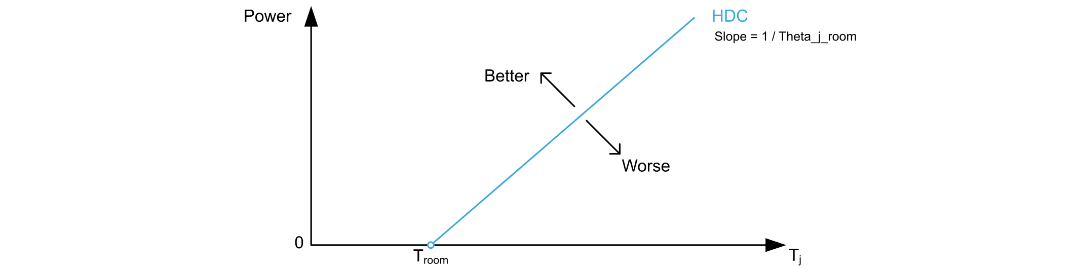
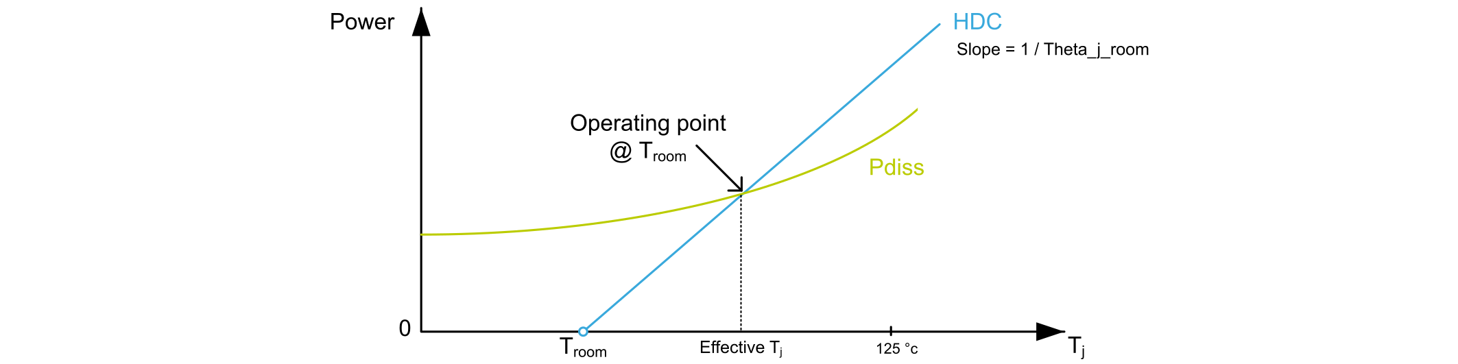
The following equation gives the heat dissipation capability (HDC):

HDC= (Tj−Troom)/(Theta_j_room)
Figure 3. HDC (heat dissipation capability)


Note:
  • Better: design has more ability to dissipate heat
  • Worse: design has less ability to dissipate heat

Case 1

The figure below shows the operating point at the intersection of the curve of the power that can be dissipated inside the design at a given TJ (HDC) and the curve of the power effectively dissipated inside the design (Pdiss).

Figure 4. HDC and junction-temperature-dependent dissipated power (case 1)

The cooling design is safe (no thermal runaway) if an intersection point exists for Troom = Troom_max, with a junction temperature < 125 °C.

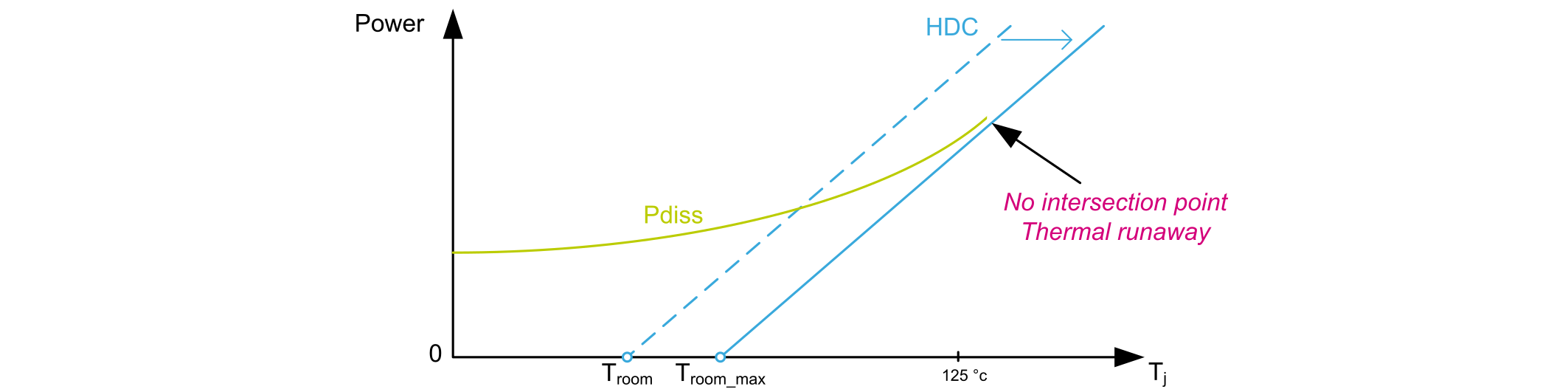
Case 2

The figure below shows the effect of an increased room temperature (without changing any other factors).
Figure 5. HDC and junction-temperature-dependent dissipated power (case 2)

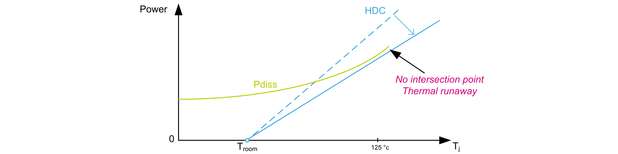
Case 3

The figure below shows the effect of an increased junction-to-room thermal resistance (without changing any other factors).
Figure 6. HDC and junction-temperature-dependent dissipated power (case 3)

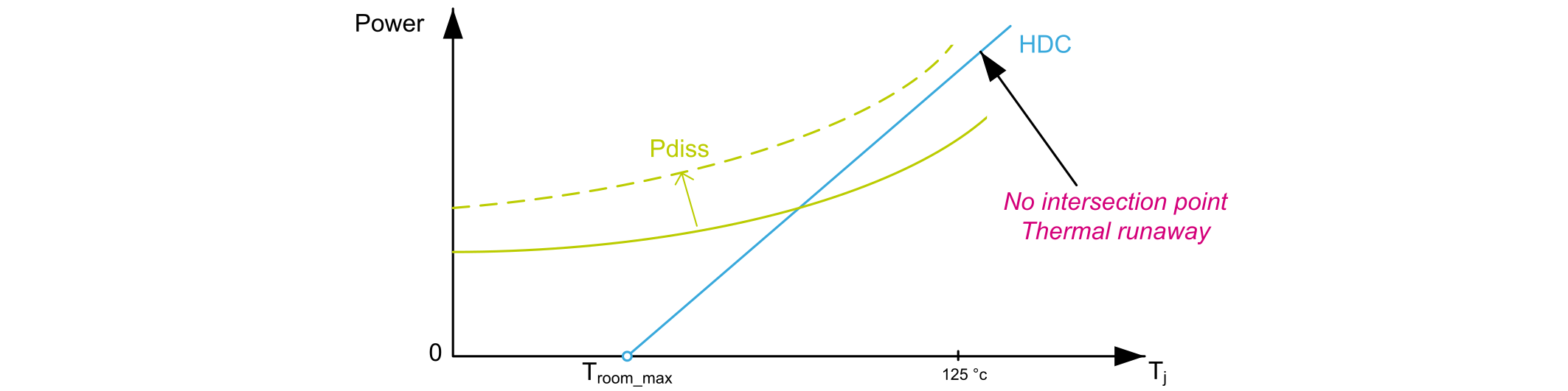
The two curves in case 2 and case 3 do not intersect. For this reason, no stable operating point is defined. This is a condition of thermal runaway.

Case 4

The figure below shows the effect of a decrease in power dissipation (without changing any other factors).
Figure 7. HDC and junction-temperature-dependent dissipated power (case 4)