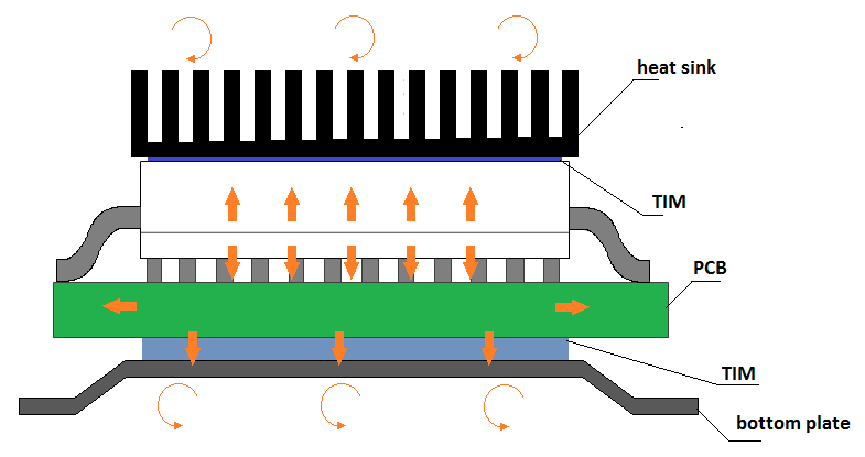
The power dissipated by the die is extracted along the two following main paths:
top side: power dissipated from the top side, (by a heat sink through an optional TIM, thermal interface material)
bottom side: power dissipated from the bottom side by the PCB, (by bottom metal plate through an optional TIM)
Figure 8. Power dissipation paths
Main cooling methods
The heat sink and the PCB dissipate the power to the surrounding environment by the convection and radiation methods.
Natural convection
The term ‘natural convection’ is used when no fan is used in the casing. This cooling method is a combination of natural convection and radiation that always work in parallel.
Forced convection
The term ‘forced convection’ is used when a fan is used in the casing.
Natural and forced convection comparison
The table below details the main comparison factors between the natural and forced convection.
Table 3. Natural and forced convection comparison
Comparison factors
Natural convection
Forced convection
Cooling efficiency
Low
Medium to high
(depending on air speed)
Cost
Low (no fan)
Higher (cost of the fan)
Reliability
Higher
(no moving parts)
Lower
(mechanical part moving)
Acoustic noise
None
Small to medium
(depending on air speed)
Possibility to control cooling efficiency based on needs
None
Yes, by varying fan voltage
Bottom cooling - host PCB design
To provide enough ‘thermal vias’, as the host PCB is a secondary heat sink for the device, it is important to use the recommended stack-up and to optimize the PCB layout beneath the package.
A significant power proportion is drawn from the package to ambient air through the host board by the paths detailed in the next sections (sorted by decreasing order of importance). The design rule implementation for ground and power connections is necessary for cooling and power distribution.
It is not possible to produce a set of rigid rules for layer construction within a PCB because each design has its own requirements.
Host PCB ground and power layout
The ground (GND) plane must have a low resistance (thermal and electrical) for all PCB areas. This improves signal quality and power dissipation. It also reduces EMI. The use of a ground layer and flooding of other layers with multiple vias maintain the resistance at a low level.
Placing as many thermal vias as possible on the ground and power planes just below the package, ensures that there is enough continuous copper between the adjacent vias for power distribution and thermal dissipation. A compromise must be found.
The possible thermal vias are listed below:
ground vias: connecting GND to the unified GND plane (these are the most efficient thermal vias)
power vias: connecting power to the power plane
The thermal vias conduct heat from the device to the internal GND and power planes. These planes spread the heat inside the PCB that acts as a planar heat sink.
Additional GND areas on outer layers
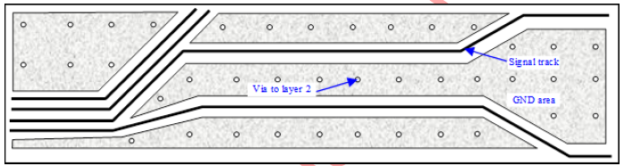
On the outer layers, some GND areas can be added wherever functional tracks are absent. Connect these areas to GND by a network of vias wherever possible.
These GND areas help in heat spreading and dissipation along the board. The figure below shows the principle of additional GND areas and vias to the GND plane.
Figure 9. Principle of additional GND areas and vias to the GND plane
Thermal analysis examples
This section shows examples of thermal analysis performed on a discovery kit (STM32H747XI MCU), an evaluation board (STM32MP157), and an internal validation board (STM32MP135 MPU).
These analyses provide some answers to the following questions (at maximum ambient temperature 85 °C):
How much does the power dissipation admit the leakage?
Is TJ < 125 °C?
Is there a risk of thermal runaway?
Discovery kit with STM32H747XI MCU
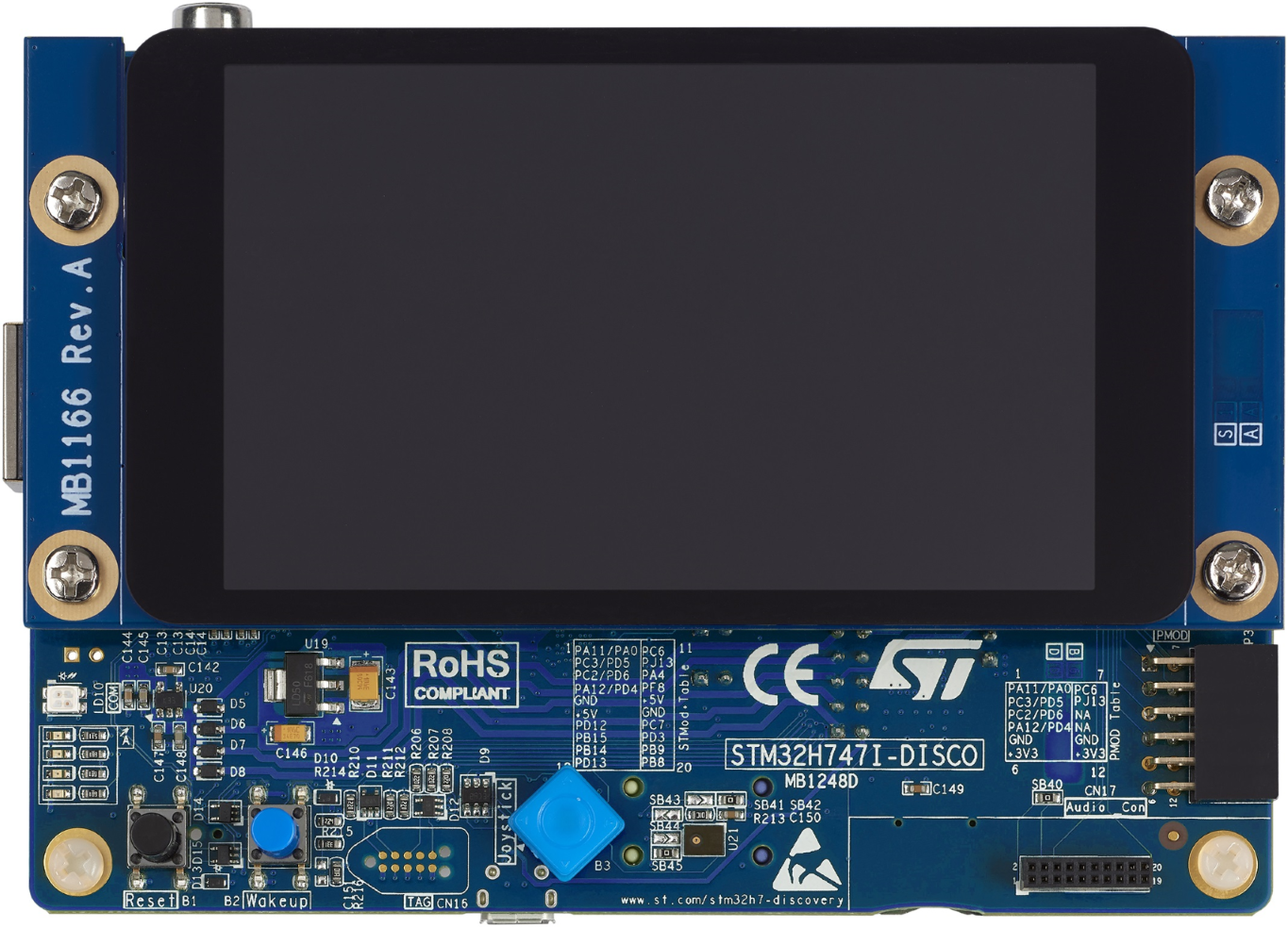
This thermal analysis has been done on a Discovery kit with an STM32H747XI device (STM32H747I-DISCO), without casing (see the figure below).
Figure 10. STM32H747I-DISCO. This picture is not contractual.
The test case is the following:
Run mode (400 MHz) data processing running from the flash memory
Cache ON
All peripherals enabled
The temperature sensor connected to the ADC3 VINP [18] input channel, is used for TJ measurement.
The TJ measurements are read via the USART2 using the DMA transfer, without CPU interruption.
STM32H7 power dissipation
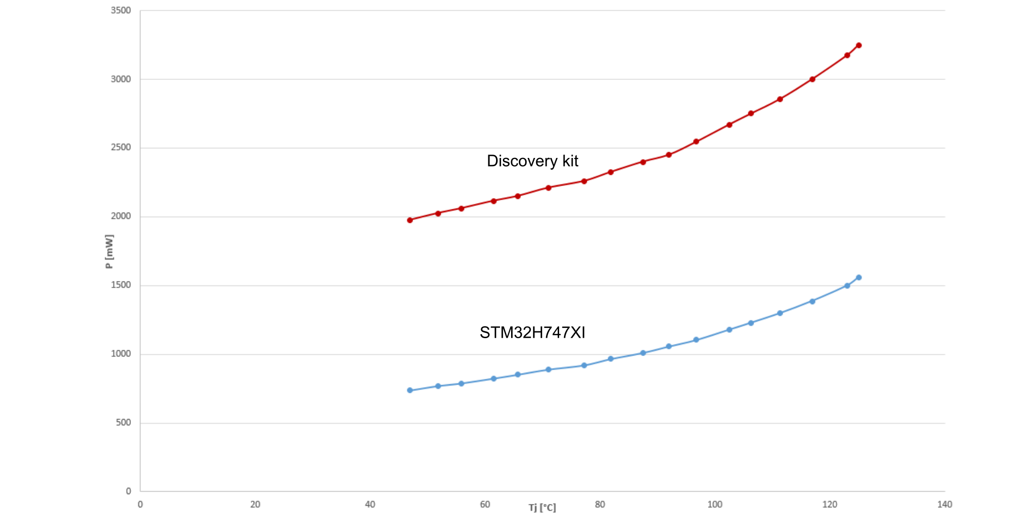
As stated in STM32 thermal parameters, the dissipated power varies with TJ. The power consumption in this example is measured for different TJ values (see the table and the figure below).
Table 4. STM32H747XI power dissipation versus Tj
TJ (°C)
STM32H747I-DISCO (supplied with 5 V)
STM32H747XI power dissipation (mW)
Current consumption (A)
Power consumption (mW)
46.9
0.395
1975
737
51.8
0.405
2025
769
55.8
0.412
2060
788
61.5
0.423
2115
824
65.7
0.430
2150
852
71
0.442
2210
888
77.3
0.452
2260
920
81.9
0.465
2325
965
87.5
0.480
2400
1010
92
0.490
2450
1056
96.8
0.509
2545
1104
102.5
0.534
2670
1179
106.3
0.550
2750
1229
111.3
0.571
2855
1298
116.9
0.600
3000
1387
123
0.635
3175
1499
125
0.650
3250
1559
Figure 11. Junction-temperature-dependent dissipated power for STM32H7
STM32H7 thermal measurements at TA = 25 °C
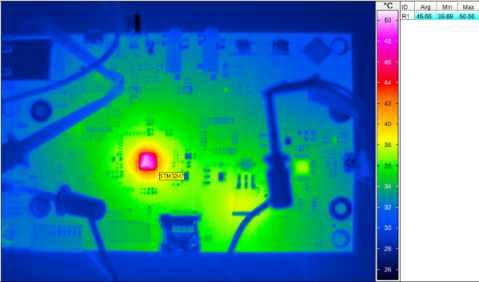
The figures and table below detail the thermal measurements performed at TA = 25 °C.Figure 12. STM32H747XI thermal measurements at TA = 25 °C
Table 5. STM32H7 thermal measurements at TA = 25°C
TJ (°C)
Thermal camera module measurement (°C)
STM32H7 power consumption (mW)
Total power consumption (mW)
Avg
Min
Max
46.9
45.5
39.7
50.6
737
1975
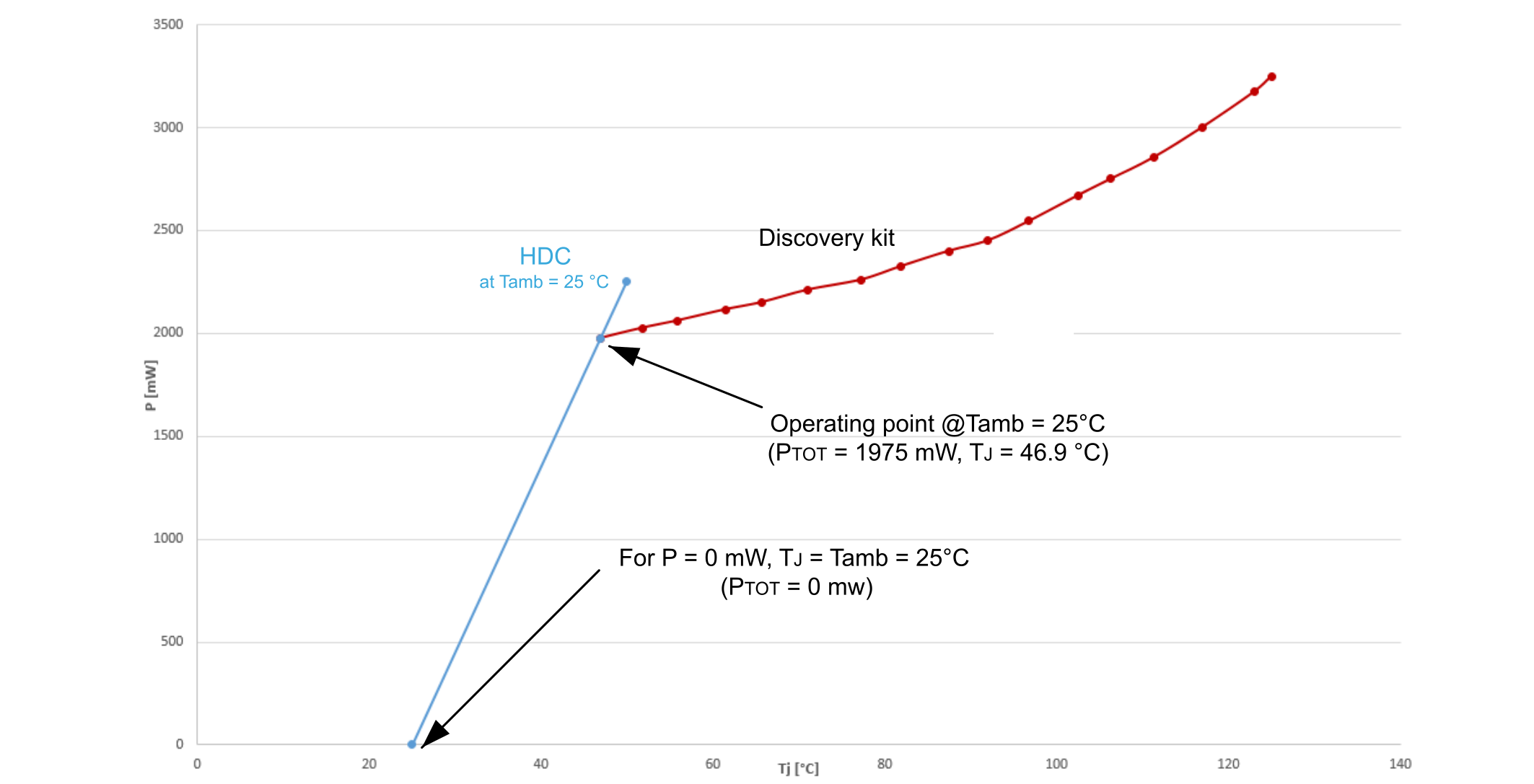
Figure 13. HDC at 25 °C and junction-temperature-dependent dissipated power for STM32H7
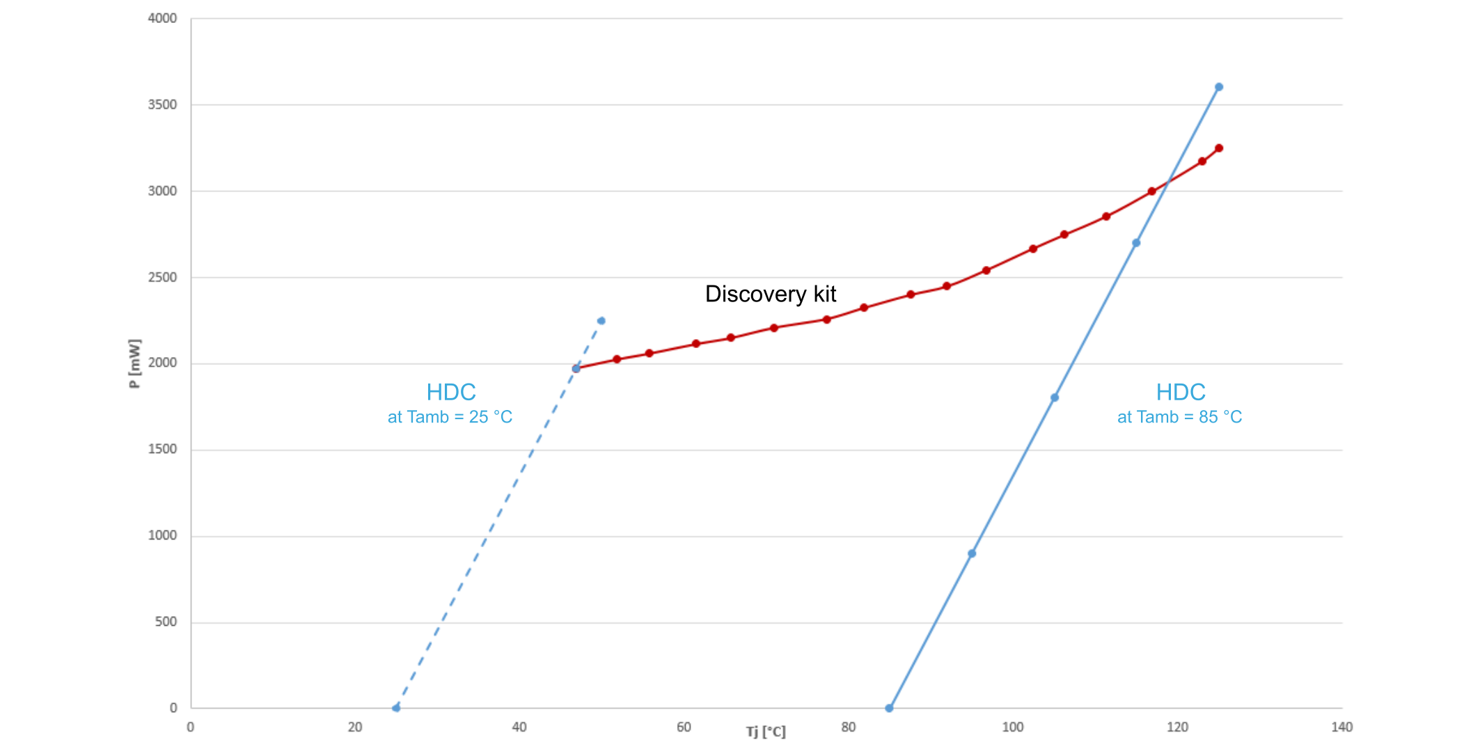
Once the design HDC is defined (by measurement at 25 °C), and assuming that this HDC is constant at 25 °C and 85 °C, the operating point of the design at 85 °C is given by translating the HDC at 85 °C. See the figure and table below.Figure 14. HDC at 85 °C and junction-temperature-dependent dissipated power for STM32H7
Table 6. Measurement interpolation at TA = 85 °C for STM32H7
Parameter
Value
TJ
119 °C
PTOT
3050 mW
In conclusion, the STM32H7 device is safe, with no thermal runaway, and TJ remaining < 125 °C.