Main differences between external and emulated EEPROM
Main differences between external and emulated EEPROM
EEPROM is a key component of many embedded applications that require nonvolatile storage of data updated with byte, half-word, or word granularity during runtime. However, microcontrollers used in these systems are very often based on embedded flash memory. To eliminate components, save PCB space and reduce system costs, the STM32 flash memory may be used instead of the external EEPROM to store not only code, but also data.
Special software management is required to store data in embedded flash memory. The EEPROM emulation software scheme depends on many factors, including the required EEPROM reliability, the architecture of the flash memory used, and the final product requirements, among other parameters.
The main differences between embedded flash memory and external serial EEPROM are the same for any microcontroller that uses flash memory technology (they are not specific to STM32 series microcontrollers). One difference is that EEPROMs do not require an erase operation to free up space before data can be written again. Other major differences are summarized in Table 2 Differences between external and emulated EEPROM.
Table 2. Differences between external and emulated EEPROM
Feature
External EEPROM (for example, M24C64: I2C serial access EEPROM)
Emulated EEPROM using on-chip flash memory
Write time
Random byte write in 4 ms. Word program time = 16 ms
Page (32 bytes) write 4 ms. Consecutive words program time = 500 μs
2 Example data for the STM32L4 series. Refer to the datasheet of your STM32 product.
Difference in write access time
Flash memories have a shorter write access time allowing critical parameters to be stored faster in the emulated EEPROM than in an external EEPROM in most cases. However, due to the data transfer mechanism, the emulated EEPROM write access time sometimes becomes significantly higher.
Programming and erase operations
Unlike flash memories, EEPROMs do not require an erase operation to free up space before writing to a programmed address. This is a major difference between a standalone EEPROM and an emulated EEPROM using embedded flash memory.
Emulated EEPROM using embedded flash memory
The erase process management is fully handled by the EEPROM emulation software, but the erase operation is left to application software management. This allows a reduction of the worst case write time, and also flash page erase operations when the application execution time becomes less critical.
Moreover, as the flash memory programming and erase operations are quite long, power failures and other spurious events that might interrupt the erase process (such as resets) have been considered when designing the flash memory management software. The EEPROM emulation software has been designed to be robust against power failures and fully asynchronous resets.
Standalone external EEPROM
Once started by the CPU, the writing of a word cannot be interrupted by a CPU reset. Only a supply failure may interrupt the write process, so power supply monitoring and properly sized decoupling capacitors are necessary to secure the complete writing process inside a standalone EEPROM.
Implementing EEPROM emulation
Principle
EEPROM emulation can be performed in various ways, considering the flash memory characteristics and final product requirements. The approach detailed below requires two sets of flash memory pages allocated to nonvolatile data.
The first set of pages is initially erased and used to store new data and flash memory programming operations are done sequentially in increasing order of flash memory addresses. Once the first set of pages is full of data, it needs to be garbage-collected.
The second set of pages collects only the valid data from the first set of pages and the remaining area can be used to store new data. Once the transfer of valid data to the second set of pages is completed, the first set of pages can be erased.
Each set of pages can be made up of one or several flash memory pages. For most STM32 series covered by this document, a header field that occupies the first four 64-bit words (32 bytes) of each page indicates its status, the exception being the STM32U5 series, where the header occupies the first four 128-bit words (64 bytes). Each page has five possible states:
ERASED: the page is empty (initial state).
RECEIVE: the page used during data transfer to receive data from other full pages.
ACTIVE: the page is used to store new data.
VALID: the page is full. This state does not change until all valid data is completely transferred to the receiving page.
ERASING: valid data in this page has been transferred. The page is ready to be erased.
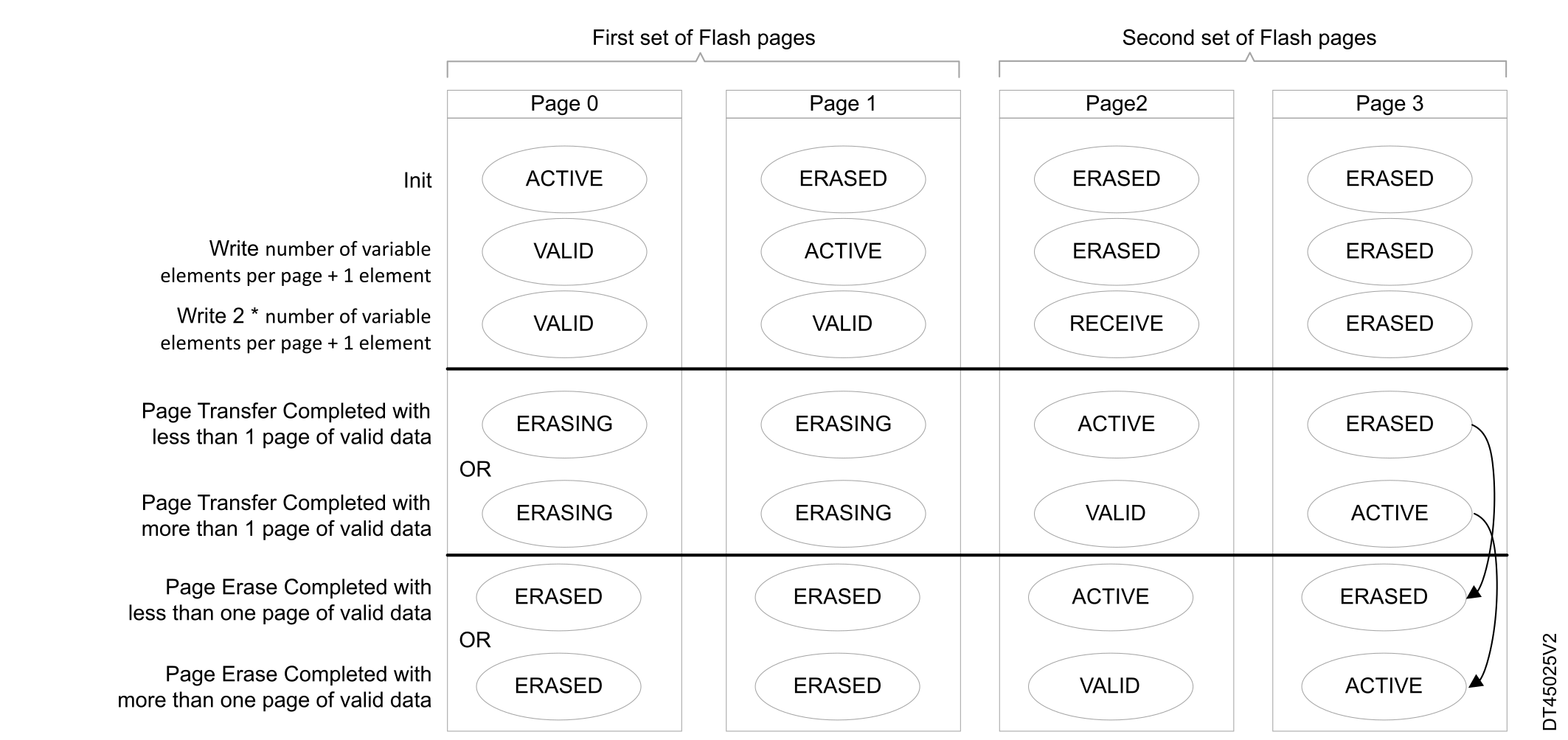
Figure 1 Page status evolution shows the page status evolution in the case where each set of pages is made of two pages.
Figure 1. Page status evolution
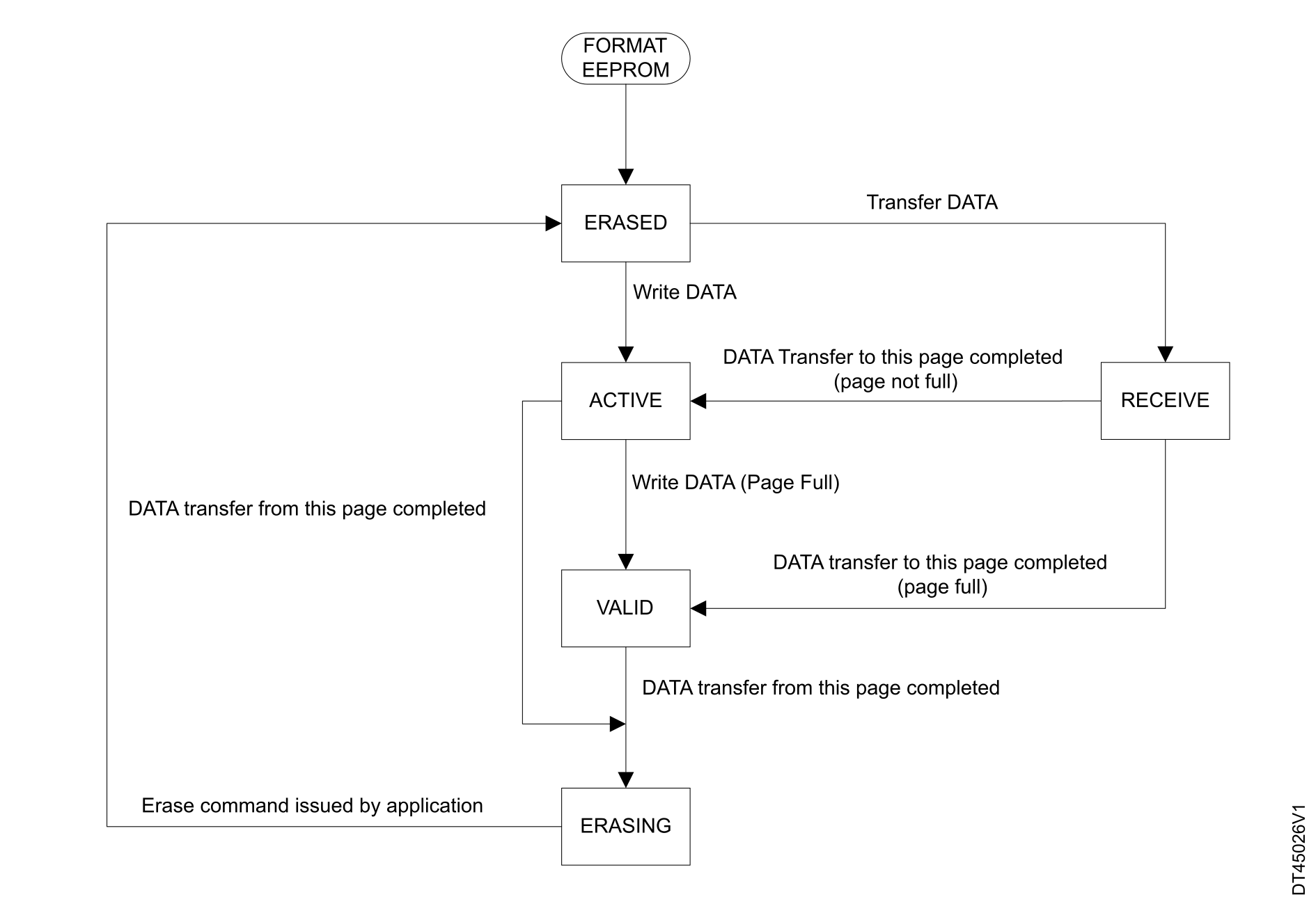
Page status valid transitions
The information provided in this paragraph is only useful for users intending to modify the EEPROM emulation driver. It is not useful for a simple utilization of the driver.
Figure 2. Page status valid transitions
Page and variable format
Depending on the STM32 series, flash memory page sizes and composition can vary.
Moreover, for some STM32 series, the EEPROM emulation driver supports either single bank mode, dual bank mode, or both. The right mode must be selected in the EEPROM emulation driver, according to the mode supported. See Table 3 Flash memory properties for this information.
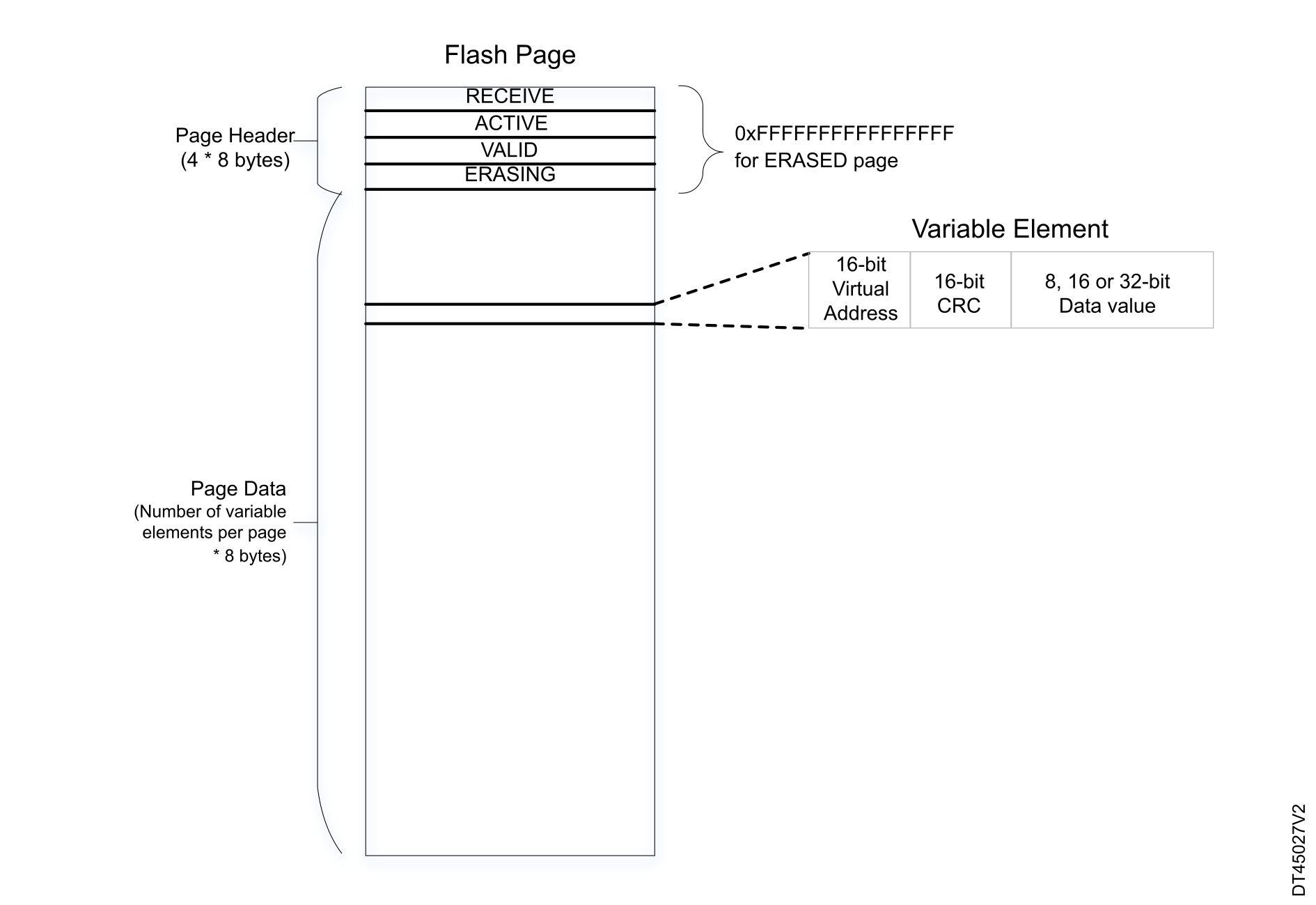
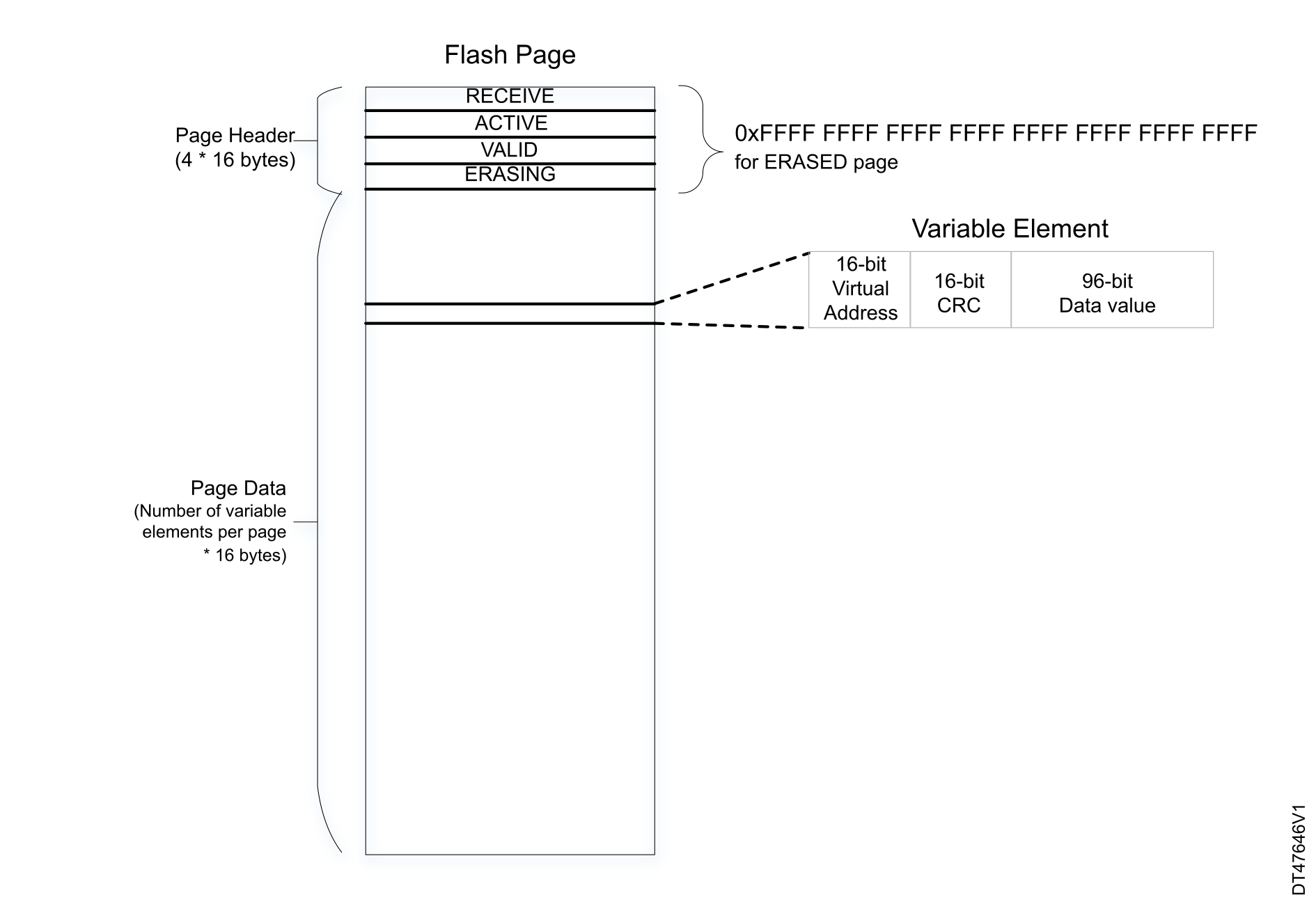
The minimal write width in flash memory is 64 bits (128 bits for STM32U5 and STM32H5 series, or 16 bits for STM32H5 series using high-cycle data area) due to its ECC (error correcting code) that cannot be switched off. Only zeros (0x0000 0000 0000 0000, or 0X0000 0000 0000 0000 0000 0000 0000 0000 for STM32U5 series) can be written to an already programmed nonnull flash memory line. As the first four words are used by the header, a flash memory page can store up to 252 variable elements when the page size is 2 Kbytes, and up to 508 variable elements when the page size is 4 Kbytes.
The possible states of a flash memory page are coded by writing 0xAAAA AAAA AAAA AAAA (or 0xAAAA AAAA AAAA AAAA AAAA AAAA AAAA AAAA for the STM32U5 series) into the page header. It is possible to determine the page state using the following procedure:
The page is in the ERASING state if its fourth line is not erased.
The page is in the VALID state if the third line is not erased and the fourth line is erased.
The page is in the ACTIVE state if the second line is not erased and the third and fourth lines are erased.
The page is in the RECEIVE state if the first line is not erased and the second, third, and fourth lines are erased.
The page is in the ERASED state if the first four lines are erased.
This algorithm allows the coding of all states and transitions described in Page status valid transitions. Each variable element is defined by a virtual address and a data value to be stored in flash memory for subsequent retrieval or update. In the implemented software, the virtual address is 16 bits long and the data value is either 8 bits, 16 bits, or 32 bits long. The driver requires the virtual address values to be between 0x0001 (0x0000 corresponds to an EEPROM element invalidated by the driver), and the maximum number of EEPROM variables required. Also, since virtual addresses are 16-bits wide, the maximum number of EEPROM variables cannot exceed 0xFFFE (0xFFFF corresponds to an erased flash memory line). Moreover, the number of variables is limited by the size of the product flash memory (see Computing the required size of flash memory for EEPROM emulation).
Each element also contains a 16-bit CRC that is used to check the element integrity. When data is modified, the modified data associated with the same virtual address is stored in a new flash memory location. Data retrieval returns the up-to-date data value.
Figure 3. Flash page and EEPROM variable format (except STM32U5 series) Figure 4. STM32U5 series Flash page and EEPROM variable format
1 When in single bank mode, these devices operate 128 bits wide read accesses. However, the EEPROM emulation solution is designed for 64 bits wide read accesses.
2 The high-cycle data area is available on the STM32H563/H573 and the STM32H562 MCUs.