AN4894 · Application noteHow to use EEPROM emulation on STM32 MCUs
Download .pdfOpen in the full document

Simple use case

Simple use case

The following example shows the software management for three EEPROM variables with the virtual addresses shown in Table 4 Emulated EEPROM virtual addresses.

Table 4. Emulated EEPROM virtual addresses
VariableVirtual addressData width
Var10x000132-bit
Var20x200032-bit
Var30x777716-bit

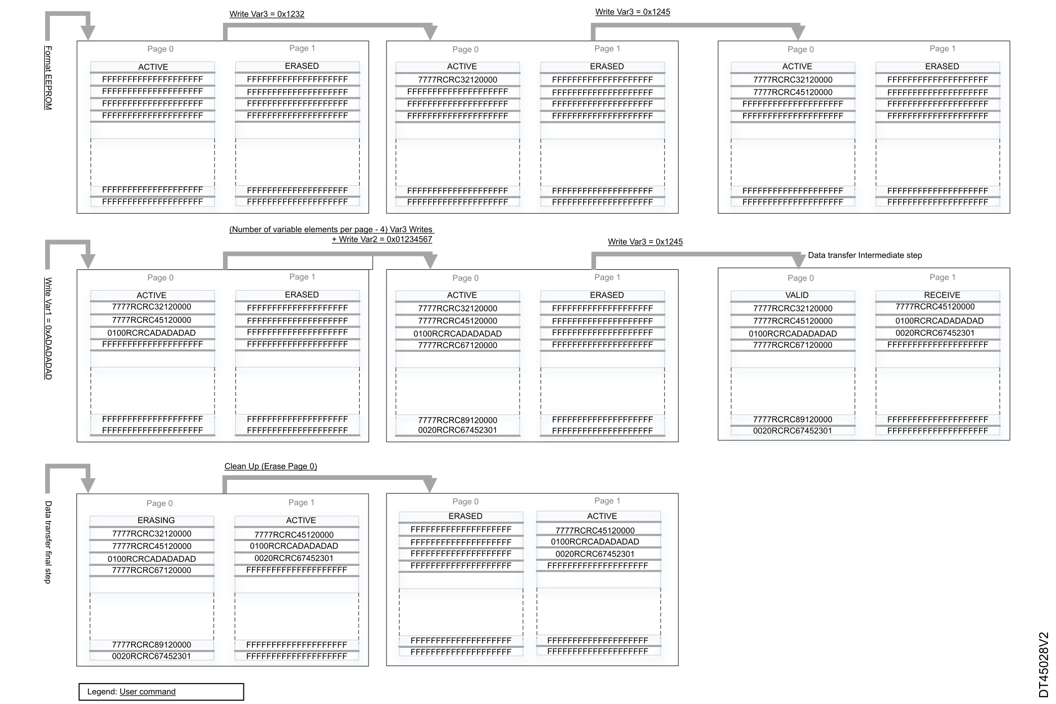
For this example, only two flash memory pages are necessary: Page 0 and Page 1. In Figure 5 Data update flow, RCRC represents the 16-bit CRC value for this variable element (refer to EEPROM emulation robustness for more details about CRC).

Figure 5 Data update flow shows only the write commands, which are done sequentially in increasing order of flash memory addresses.

Figure 5. Data update flow


Reading data

Read commands perform flash memory reads from the highest to the lowest address in the ACTIVE or VALID page, and return only valid data. Data is considered valid if it is the latest to be written at a given virtual address, and the integrity check using CRC passes.

Note:

Only valid data is copied during the data transfer mechanism.

Advanced features

The EEPROM emulation firmware is designed to fulfill most of the requirements for an embedded application in terms of nonvolatile storage. This section covers these requirements in detail. Other embedded application requirements may be needed in particular cases and are addressed in Embedded application aspects.

Data granularity management

Emulated EEPROM can be used in embedded applications where nonvolatile storage of data updated with a byte, half-word, or word granularity is required. Data size generally depends on application requirements such as sensor or communication-interface data size.

The EEPROM emulation firmware is designed to support byte, 16-bit half-word, and 32-bit word granularity (96-bit word granularity for STM32U5 series). However, to optimize the flash memory usage, the user application can gather all smaller sized data elements into 32-bit data elements before storing the content in emulated EEPROM. This would ensure an optimal use of the 64-bit flash memory line by simultaneously writing the 16-bit virtual address, the 16-bit CRC, and the 32-bit data value.

Conversely, it is possible to write the 32-bit data value on two 16-bit half-word with the 16-bit virtual address and the 16-bit CRC, allowing a 32-bit data granularity in the high-cycle data area available in STM32H5 series, which only supports 16-bit half-word granularity by line.

For STM32U5 and STM32H5 series, the user can gather all smaller sized data elements into 96-bit data elements before storing the content in emulated EEPROM. This ensures optimal use of the 128-bit flash memory line by simultaneously writing the 16-bit virtual address, the 16-bit CRC, and the 96-bit data value.

Note:

The minimal write width in flash memory is 64 bits (128 bits for STM32U5 and STM32H5 series, or 16 bits for STM32H5 series using high-cycle data area) due to its ECC (error correcting code), commands, which cannot be switched off.
Wear leveling algorithm and flash memory page allocation

A wear leveling algorithm allows monitoring and even distribution of flash memory write and erase operations between flash memory pages. When no wear-leveling algorithm is used, the pages are not used at the same rate. For instance, pages with long-lived data do not endure as many write and erase cycles as pages that contain frequently updated data. The wear-leveling algorithm ensures that equal use is made of all the available write cycles for each flash memory page.

By design, the EEPROM emulation algorithm distributes evenly the flash memory write and erase operations between flash memory pages. Flash memory writes are performed sequentially in increasing-address order whatever user variable is written. When one set of pages is full, the valid elements are copied to the other set of pages, and the first set of pages is fully erased.

Guard pages

To even further reduce wear on flash memory pages, the user can decide to add an even number of flash memory guard pages (one guard page per set of pages by default). No guard page is necessary if the number of emulated variables leaves significant room in the ACTIVE page. Increasing this number (4,6,...) increases the flash memory endurance beyond the enabled value. This feature is closely linked to the emulated EEPROM cycling capability - refer to paragraph Cycling capability: EEPROM endurance improvement.

Taking an example based on the STM32L4, an emulation of 1000 EEPROM variables can be stored in two sets of four flash memory pages (each page being able to store 252 elements). When all elements are written once (or after a page transfer), only eight more elements can be written before a new page transfer is triggered. In this case, the addition of two guard pages is recommended (one per set of pages) so that 260 writes can be performed before a new page transfer is triggered.

Cycling capability: EEPROM endurance improvement

When EEPROM technology is used, each byte can be individually programmed a finite number of times (typically in the range of 1 million). When flash memory technology is used, it is not possible to write to a nonerased address, and the minimum erase size is the flash memory page size. Consequently, we need to define a program/erase cycle that consists of several flash memory line write accesses followed by one flash memory page erase operation.

Each STM32 device on-chip flash memory page can be programmed and erased reliably a limited number of times. For write-intensive applications that need to update each variable more than this number, the wear leveling algorithm allows the endurance of the emulated EEPROM to be increased.

Table 5 Flash memory endurance shows the limit number of reliable programming and erasing operations for devices covered by this application note:

Table 5. Flash memory endurance
STM32 seriesFlash memory endurance
STM32L4 series10 kcycles
STM32L4+ series10 kcycles
STM32L5 series10 kcycles
STM32G0 series10 kcycles (1 kcycles for STM32G030x6/x8 and STM32G070CB/KB/RB)
STM32G4 series10 kcycles
STM32WB series10 kcycles
STM32WL series10 kcycles
STM32U0 series10 kcycles
STM32U3 series10 kcycles
STM32U5 series

10 kcycles endurance on all flash memories
100 kcycles on up to 256 Kbytes per bank

STM32C0 series10 kcycles
STM32H5 series

10 kcycles on all flash memories
100 kcycles in high-cycle data area

Knowing the requested size of emulated EEPROM and the targeted endurance, it is possible to compute the flash memory size to be used for that purpose. The flash memory size is also a function of the data width of stored variables.

Table 6. Flash usage for a 4000-byte emulated EEPROM (STM32L4/L4+)
Data widthNumber of pages needed for 10 kcycles enduranceFlash size for 10 kcycles enduranceNumber of pages needed for 100 kcycles enduranceFlash size for 100 kcycles endurance
STM32L4
8-bit3468 Kbytes3226441 Kbytes
16-bit1836 Kbytes162324 Kbytes
32-bit1020 Kbytes82164 Kbytes
STM32L4+
8-bit1872 Kbytes162648 Kbytes
16-bit1040 Kbytes82328 Kbytes
32-bit624 Kbytes42168 Kbytes
Note:

To get the same information for other STM32 series, you can apply the formula presented in Computing the required size of flash memory for EEPROM emulation.

1 Not applicable for STM32L4: a maximum of 512 Kbytes can be allocated to EEPROM emulation. Refer to the STM32 product datasheet for the size of each bank.