AN4894 · Application noteHow to use EEPROM emulation on STM32 MCUs
Download .pdfOpen in the full document

High-cycle data area of flash memory

High-cycle data area of flash memory

The embedded flash memory of STM32H563/H573 and STM32H562 MCUs offers up to 96 Kbytes (maximum) memory area with high cycling capability (100 kcycles) to store data and emulate EEPROM. It can be accessed through the AHB system port from the following address: 0x0900_0000 to 0x0901_7FFF. It is mapped in the eight (or four) last sectors of Bank1 and 2. This area is protected by a robust 6-bit ECC, which enables a read and write granularity of 16 bits at the expense of having sector size shrunk to 6 Kbytes.

A threshold per bank (EDATA(1/2)_STRT) is programmable in user option bytes to determine the beginning of the data flash area. By default, all flash memories are used for code. For example, if 48 Kbytes of data are needed in Bank1, set EDATA1_EN to 1, and EDATA1_STRT to 7. If no data are needed in Bank2, set EDATA2_EN to 0. In this case, the data are accessible from address 0x0900_0000 to 0x0900_BFFF for Bank1. For greater efficiency, it is always recommended to use sector on the other bank for flash memory high-cycle data, so that the application benefits from the RWW capability of the dual-bank arrangement. When the SWAP_BANK feature is enabled, the banks are swapped. The flash memory high-cycle data in Bank 2 are accessible from 0x0900_000 to 0x0900_BFFF, and the data in Bank 1 are accessible from 0x0900_C000 to 0x0901_7FFF.

A bus error is generated on:

  • Attempt to access an address between 0x0900_0000 to 0x0901_7FFF while this address is not valid (EDATA(1/2)_EN not enabled or EDATA(1/2)_STRT not correct).
  • Attempt to fetch instructions from flash memory high-cycle data area. Erasing the data area sector is possible by normal erase request for the corresponding user flash memory sector (120-127).
Note:

More information about the high-cycle data area and its protections are documented in AN4894_General-information.html#id_60716__entry_a2h_xy5_11c
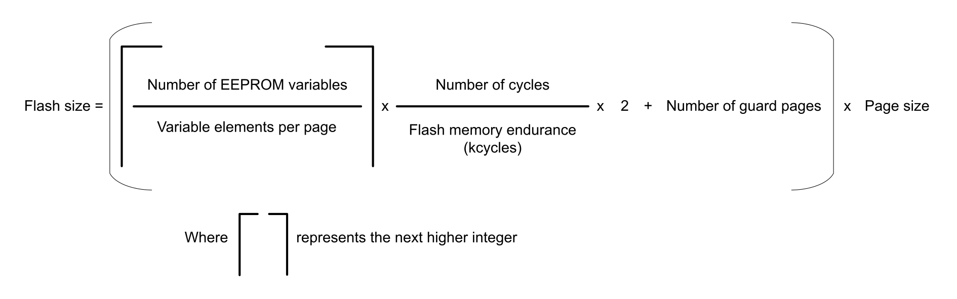
Computing the required size of flash memory for EEPROM emulation

As first approximation, the required size of flash memory is proportional to the emulated EEPROM size and to the cycling capability. Table 6 Flash usage for a 4000-byte emulated EEPROM (STM32L4/L4+) can be used to estimate the required size of flash memory according to the data width of stored elements for STM32L4 series and STM32L4+ series MCUs.

For a precise flash memory size requirement, whatever the STM32 series, use the formula below:

Note:

Values of ‘flash memory endurance values (kcycles)’ for applicable STM32 series are listed in Table 5 Flash memory endurance.

The formula is decomposed into the following steps:
  1. Knowing the number of elements a flash memory page can store (refer to Table 3 Flash memory properties) compute the number of flash memory pages needed to store the EEPROM elements. The calculated flash memory size is independent of the element data width.
  2. Multiply the number of pages by the targeted integer cycling ratio, for instance 1 for the standard 10 kcycles endurance or 10 to achieve 100 kcycles endurance when the flash memory endurance is 10 kcycles. The flash memory endurance of the product indicated in Table 5 Flash memory endurance must be considered.
  3. Multiply the number of flash memory pages by 2 to include the data transfer mechanism.
  4. Add the number of guard pages (an even number) to get the final number of flash memory pages.
  5. Knowing the flash memory page size for your product (refer to Table 3 Flash memory properties), compute the flash memory size required by the EEPROM emulation.

STM32L4 calculation example

To store 4000 individual bytes, and knowing that each page can store up to 252 elements, a set of pages must comprise 16 flash memory pages. A second set of pages, of the same size, is required to transfer data when the first one is full. If we assume that we use two guard pages, 34 flash memory pages are necessary.
Note:

This calculation is a slightly conservative estimation.

EEPROM emulation robustness

In an embedded application, it is possible that a power failure or asynchronous reset might occur while programming or erasing the flash memory. In this case, the content of the flash memory line (if programming) or the complete flash memory page (if erasing) is unknown. There can be a single- or a multiple-bit error, with or without error correcting code detection (ECCD) or correction (ECCC).

Note:

Note: The hardware ECC is designed to detect and correct errors after flash memory wear, but not to detect flash memory program or erase operation interruptions reliably. ECC is not available on STM32C0 series.

The EEPROM emulation software is designed and validated to be robust against power failures and asynchronous resets. This robustness relies on several features in the flash memory interface and EEPROM emulation driver that are detailed in the following paragraphs. Refer to the product errata sheet for the flash memory limitations and workarounds.

Data recovery

To detect corrupted data (virtual address and/or data value), a 16-bit CRC (cyclic redundancy check) has been implemented. It is based on the ANSI CRC-16 with the following polynomial: x15 + x2 + 1 (represented as 0x8005). Even though this polynomial offers a very high detection rate, it can be modified by the user in the EEPROM configuration file.

When writing a variable element, it is stored with its corresponding CRC value. When reading or transferring a variable element, the CRC is computed and checked against the value stored in the variable element. If it matches, the variable element is considered as valid. In the case of a mismatch, the variable element is invalidated.

Note:

The CRC peripheral is used by the EEPROM emulation software to accelerate the CRC computation.

The data recovery feature relies on the fact that all-zeros, and only a full 64-bit zero (128 for STM32U5 series), can be written to an already programmed nonnull word. Invalidating a variable element is done by writing zeros in the variable element. As a consequence, this precludes the use of 0x0000 as a virtual address for the variable element.

Note:

The virtual address 0xFFFF is also forbidden as it corresponds to an erased flash memory line.

The data recovery mechanism also requires the user to write zeros in case an ECCD NMI is triggered on this flash memory line. This is achieved by calling the FI_DeleteCorruptedFlashAddress function from the NMI service routine in case the ECC detects an error that it cannot correct (that is, the ECCD bit is set).

This mechanism is only applied during the cleanup phase operated in the EE_Init function. After this phase, it is assumed that there are no further NMI trigger events.

It is possible that, for some reason, the zero programming operation fails and that a flash memory programming error flag (PROGERR, PGAERR, or PGSERR) is raised (for example if the flash memory line was already at 0, PROGERR is raised). The line then is considered invalid and is kept in its current state (the NMI service routine exits without doing anything).

If flags other than PROGERR, PGAERR or PGSERR are set, the NMI routine enters an infinite loop.

If, despite the cleanup phase, another NMI is triggered during the EEPROM emulation, nothing is done. The fact that the NMI is raised is considered to invalidate the line. The cleanup phase eliminates the majority of lines corrupted by an asynchronous reset or power down. Thus, after the cleanup phase, the number of remaining NMIs may, in most cases, be 0.

If during the first write to a variable element with a given address, the write is interrupted by a power failure or an asynchronous reset, the driver considers that there is no data at this address. In all other cases, the EEPROM emulation software always returns the latest valid data value by finding the previous value for this data stored in flash memory.

Page header recovery

Similarly to data corruption, the page header can be corrupted in the case of power loss or asynchronous reset during a header update or a flash memory page erase.

To detect this corruption and recover from it, the EE_Init routine is implemented. It is called immediately after power-up. This routine checks the sequence of page statuses for integrity and performs a repair if necessary. This ensures that no data is lost. Refer to EEPROM emulation timing for more details.

To avoid a possible failure scenario, erased pages are systematically erased again upon reset (in the EE_Init routine). This ensures a safe behavior but consumes cycling capability of the emulated EEPROM. This systematic erase can be avoided if the application is designed not to generate an asynchronous reset or power failure during flash memory writes or erases. Refer to Detecting power failures for more details.

Robustness is achieved at the expense of several checks and recovery mechanisms implemented in the EE_Init routine. This induces a slight code size increase and longer initialization time when compared with simpler EEPROM emulations. See EEPROM emulation timing for further details.

Real-time considerations

The provided implementation of the EEPROM emulation firmware runs from internal flash memory, thus accesses to the same flash memory bank are stalled during flash memory erase or programming operations (EEPROM initialization, variable update, or page erase).

As a consequence, the application code is not executed and interrupts cannot be served during a maximum time equal to the longest page-erase operation duration for your STM32 product (see the applicable datasheet). This behavior may be acceptable for many applications, however for applications with real-time constraints, the user needs to take corrective action.

Device embedding flash memory with RWW (read while write) capability

With STM32 devices embedding a dual-bank flash memory, it is recommended to put the critical routines (vector table, critical interrupt service routines) in one bank and the area used for EEPROM emulation in the other bank. The flash memory area in the bank used for EEPROM emulation can still be used, but with execution delays during flash memory write and erase operations.

Note:

To know whether your STM32 device supports flash memory with RWW capability, refer to the product datasheet.

Running the critical processes from the internal RAM

Another way to fulfill real-time constraints is to run the critical code from internal RAM:

  1. Relocate the vector table into the internal RAM.
  2. Execute all critical processes and interrupt service routines from the internal RAM. The compiler provides a keyword to locate the functions in RAM. The functions are copied from the flash memory to the RAM at system startup just like any initialized variable.
Note:

It is important to note that for a RAM function, all used data, and called functions need to be located within the RAM.

Dual core considerations

On some STM32 devices, two cores are available (refer to the applicable STM32 product datasheet and reference manual for more information). This is the case for a majority of the products from the STM32 wireless series for example.

STM32WB series MCUs integrate a main core (CPU1, Arm Cortex-M4) alongside a second core (CPU2, Arm Cortex-M0+) that is dedicated to radio. Here we consider an example in a radio context, where CPU1 runs the EEPROM emulation and needs to process a flash memory operation.

To achieve this while avoiding conflicts with CPU2, CPU1 must check that the radio application running on CPU2:
  • is not currently accessing flash memory.
  • does not urgently need to access flash memory.
Note:

Erase operations in particular take a relatively long time regarding the radio protocol specifications. Therefore, a mechanism must also be implemented to avoid the start of a long CPU1 operation (such as an erase) if CPU2 has already planned an urgent flash memory operation.

Application developers adapting the EEPROM emulation application for a dual-core product may need to implement these verifications.

For instance, for STM32WB series MCUs it is possible to use the following features:
  • The hardware semaphore feature (HSEM)
  • The CRPF bit from the PWR_EXTSCR register bit (set when a critical radio operation is ongoing)

Both are available on STM32WB series MCUs.

Note:

The same problematic applies to some dual-core applications other than radio.

For STM32WB series products integrating a Bluetooth® LE stack, a ‘flash access management’ mechanism, based principally on the hardware semaphore feature, is described in document AN4894_General-information.html#id_60716__entry_azg_btt_szb.

For the P-NUCLEO-WB55 Nucleo board, two examples are provided in the X-CUBE-EEPROM firmware package (see STM32Cube expansion software (X-CUBE-EEPROM)):
  • An example that simply exploits the EEPROM emulation driver (similar to the examples for other series).
  • An example that maintains a Bluetooth® LE connection and communication while processing EEPROM operations. It follows the flash memory access timing rules in document AN4894_General-information.html#id_60716__entry_azg_btt_szb, and can be used as a reference for implementing this mechanism.

To determine the availability of the above mechanisms for other STMicroelectronics MCUs with RF stacks, refer to their datasheets and other related documentation.