Power supplies
The STM32U5 devices require a 1.71 to 3.6 V operating voltage supply (VDD).
The independent supplies listed below, can be provided for specific peripherals:
- VDD = 1.71 V to 3.6 V
VDD is the external power supply for the I/Os, the internal regulator, and the system analog such as reset, power management, and internal clocks. VDD is provided externally through the VDD pins.
- VDDA = 1.62 V (ADCs/COMPs/DACs/OPAMPs) / 1.8 V (VREFBUF) to 3.6 V
VDDA is the external-analog power supply for A/D converters, D/A converters, voltage reference buffer, operational amplifiers, and comparators. The VDDA voltage level is independent from the VDD voltage. The VDDA pin must preferably be connected to the VDD voltage supply when these peripherals are not used.
Note:In case the VDDA pin is left at high impedance or is tied to VSS, the maximum input voltage that can be applied on the I/Os with "_a" I/O structure, is reduced (refer to device datasheet for more details).
- VDDSMPS = 1.71 V to 3.6 V
VDDSMPS is the external power supply for the SMPS step-down converter. It is provided externally through the VDDSMPS pin, and must be connected to the same supply as VDD pin when the SMPS is used in the application. When the SMPS is not used, it is recommended to connect both VDDSMPS and VLXSMPS to ground.
- VLXSMPSThe VLXSMPS pin is the switched SMPS step-down converter output.Note:
The SMPS output can not be used to power external components.
- VDD11
VDD11 is a digital core supply provided through the internal SMPS step-down converter VLXSMPS pin. VDD11 pins (two or three) are present only on packages with internal SMPS, connected to a total of 4.7 µF (typical) external capacitors.
- VCAPVCAP is the digital core supply, from the internal LDO regulator. VCAP pins (one or two) are present only on packages with LDO only (without SMPS), connected to a total of 4.7 µF (typical) external capacitor.Note:
- In case there are two VCAP pins (UFBGA169 package), each pin must be connected to a 2.2 µF capacitor, for a total around 4.4 µF.
- The SMPS power supply pins (VLXSMPS, VDD11, VDDSMPS, VSSSMPS) are available only on packages with SMPS. In such packages, the STM32U5 devices embed two regulators, one LDO and one SMPS in parallel, to provide the VCORE supply to digital peripherals. A 4.7 μF total external capacitor and a 2.2 µH coil are required on VDD11 pins.
- The flash memory is supplied by VCORE and VDD.
- VDDUSB = 3.0 V to 3.6 VVDDUSB is the external-independent power supply for USB transceivers. The VDDUSB voltage level is independent from the VDD voltage. The VDDUSB pin must preferably be connected to the VDD voltage supply when the USB is not used.Note:
In case the VDDUSB pin is left at high impedance or is tied to VSS, the maximum input voltage that can be applied on the I/Os with "_u" I/O structure, is reduced (refer to device datasheet for more details).
- VDD11USB = 1.0 V to 1.26 V (only available on STM32U59x/5Ax/5Fx/5Gx devices)
VDD11USB is the external power supply for the USB transceiver. This supply is only available on specific packages and must be connected to VDD11.
- VDDIO2 = 1.08 V to 3.6 V VDDIO2 is the external power supply for 14 I/Os (port G[15:2]). The VDDIO2 voltage level is independent from the VDD voltage, and must preferably be connected to VDD when PG[15:2] is not used.Note:
On small packages, VDDA, VDDIO2, or VDDUSB independent power supplies may not be present as a dedicated pin, and are internally bonded to a VDD pin. They are neither present when the related features are not supported on the product.
- VBAT = 1.55 V to 3.6 V
VBAT is the power supply when VDD is not present (through power switch) for RTC, TAMP, external clock 32 kHz oscillator, backup registers, and optionally backup SRAM.
- VREF-, VREF+
VREF+ is the input reference voltage for ADCs and DACs. It is also the output of the internal voltage reference buffer (VREFBUF) when enabled. The VREF+ pin can be grounded when ADC and DAC are not active.
The internal voltage reference buffer supports four output voltages that are configured with the VRS[2:0] field in VREFBUF_CSR register:- VREF+ around 1.5 V. This requires VDDA ≥ 1.8 V.
- VREF+ around 1.8 V. This requires VDDA ≥ 2.1 V.
- VREF+ around 2.048 V. This requires VDDA ≥ 2.4 V.
- VREF+ around 2.5 V. This requires VDDA ≥ 2.8 V.
VREF- and VREF+ pins are not available on all packages. When not available, they are bonded to VSSA and VDDA pins, respectively.
When the VREF+ pin is double-bonded to VDDA in a package, the internal VREFBUF is not available, and must be kept disabled.
VREF- must always be equal to VSSA.
- VDDDSI = 1.71 V to 3.6 V (only available on STM32U59x/5Ax/5Fx/5Gx devices)
VDDDSI is the external power supply for the DSI controller. It is provided externally through the VDDDSI supply pin, and must be connected to the same supply as VDD pin.
- VDD11DSI = 1.0 V to 1.26 V (only available on STM32U59x/5Ax/5Fx/5Gx devices)
VDD11DSI is the external power supply for the DSI transceiver and must be connected to VDD11.
The following figures present an overview of the STM32U5 devices power supply, depending on the SMPS presence.
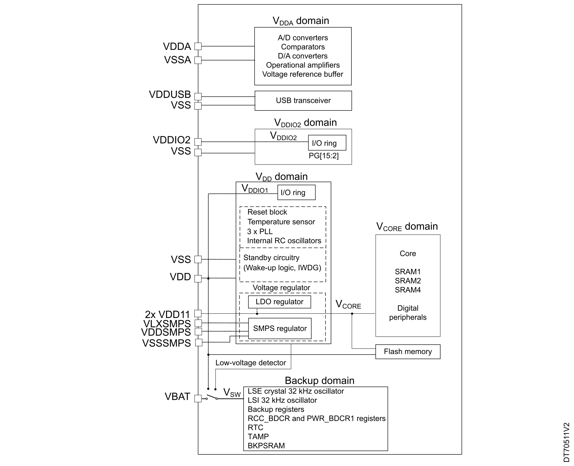
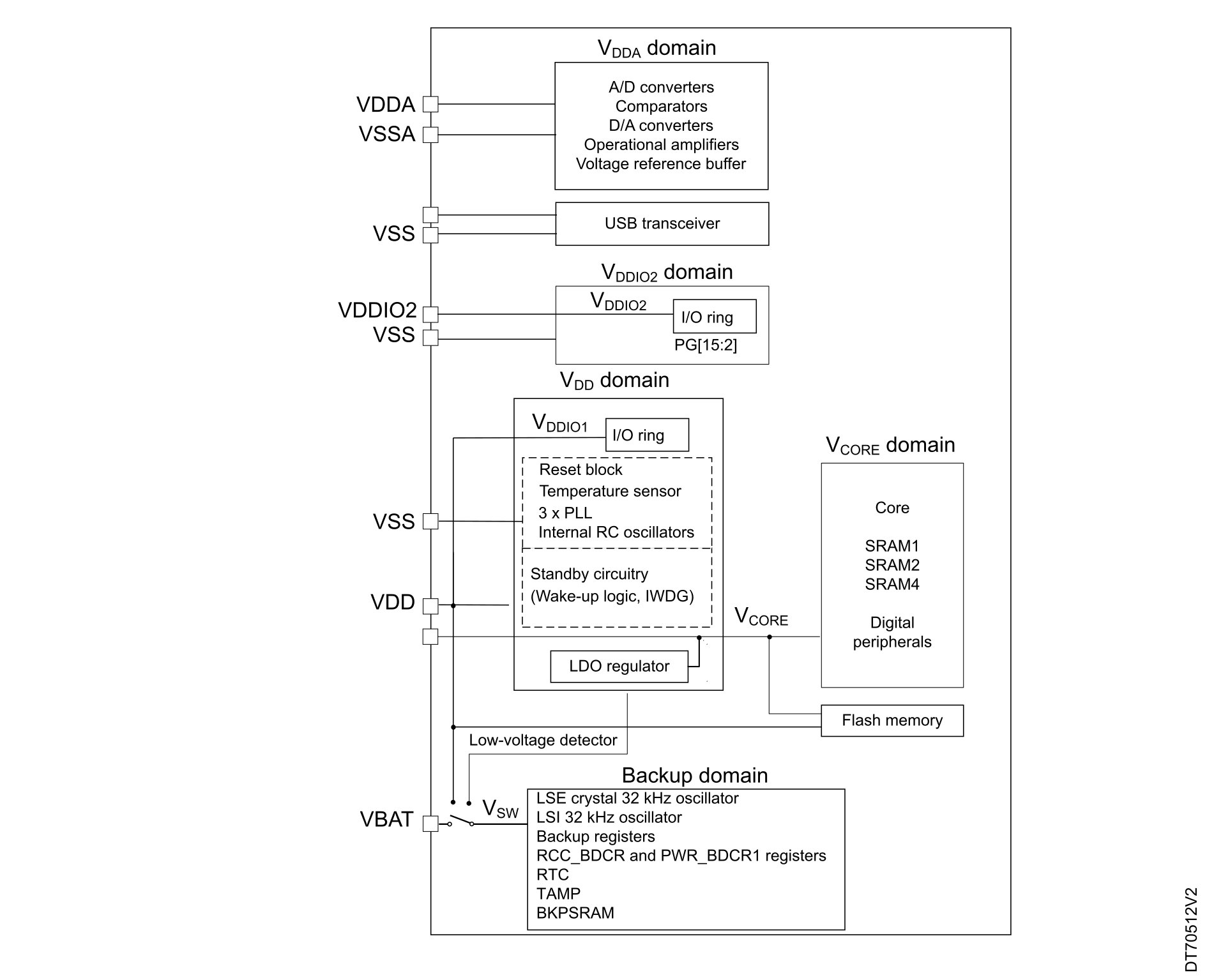
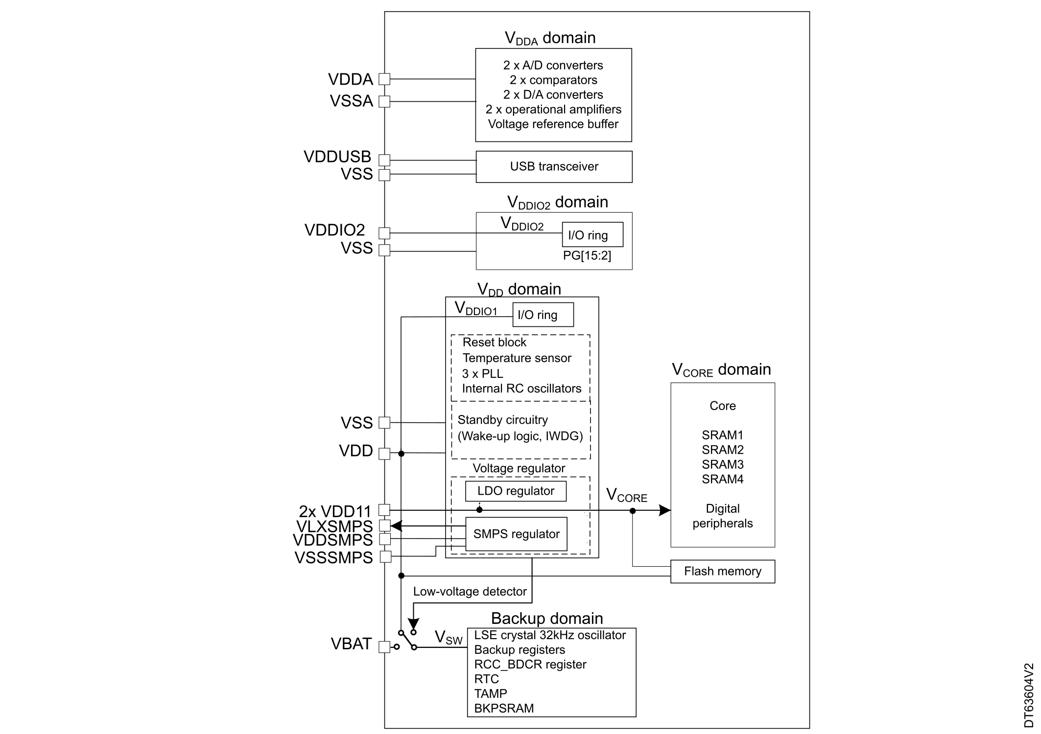
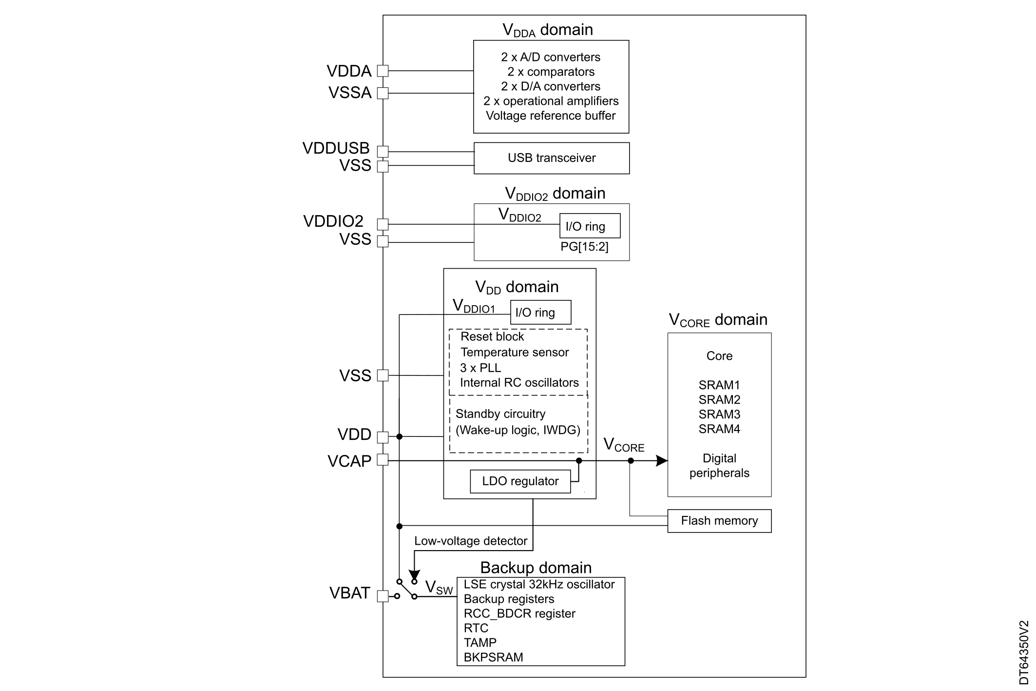
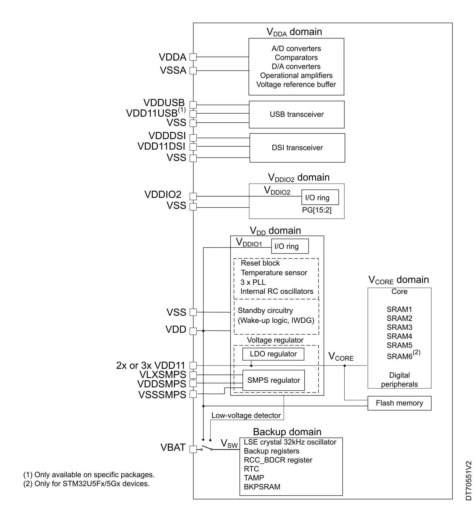
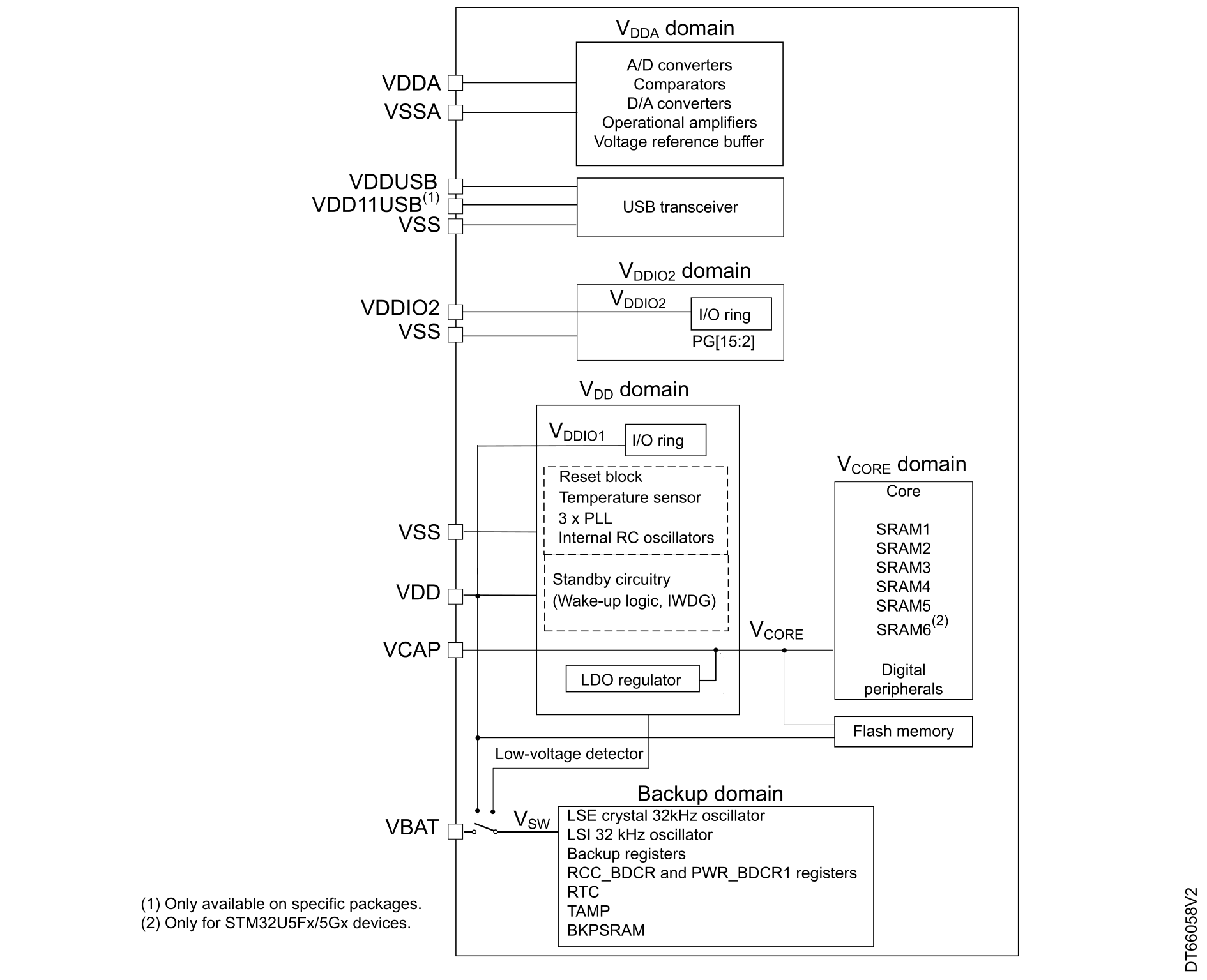
In devices without SMPS, the VDD supply source feeds the I/Os and system analog peripherals (such as PLLs and reset block). The VCORE power supply for digital peripherals and memories is generated from the LDO.
Note: If the selected package has the SMPS step-down converter option but the SMPS is not used by the application (and the embedded LDO is used instead), the SMPS power supply pins must be set as follows:
- VDDSMPS and VLXSMPS connected to VSS
- VDD11 pins connected to VSS through two 2.2 µF capacitors as in normal mode
Independent analog peripherals supply
To improve ADC and DAC conversion accuracy and to extend the supply flexibility, the analog peripherals have an independent power supply that can be separately filtered and shielded from noise on the PCB.
The voltage supply input of the analog peripherals is available on a separate VDDA pin. An isolated supply ground connection is provided on VSSA pin.
The VDDA supply voltage can be different from VDD. After reset, the analog peripherals supplied by VDDA are logically and electrically isolated and therefore are not available. The isolation must be removed before using these peripherals, by setting the ASV bit in PWR_SVMCR, once the VDDA supply is present.
The VDDA supply can be monitored by analog voltage monitors (AVM), and compared with two thresholds (1.6 V for AVM1 or 1.8 V for AVM2). For more details, refer to the device datasheet and section Peripheral voltage monitoring (PVM) of document AN5373_general-info.html#id_14462__entry_msl_1fh_dvb.
When a single supply is used, the VDDA pin can be externally connected to the same VDD supply, through an external filtering circuit, to ensure a noise-free VDD reference voltage.
ADC and DAC reference voltage
To ensure a better accuracy on low-voltage inputs and outputs, the user can connect to VREF+ pin, a separate reference voltage lower than VDDA.
VREF+ is the highest voltage, represented by the full-scale value, for an analog input (ADC) or output (DAC) signal. VREF+ can be provided either by an external reference or by the VREFBUF that can output a configurable voltage: 1.5, 1.8, 2.048 or 2.5 V. The VREFBUF can also provide the voltage to external components through the VREF+ pin.
For further information, refer to the device datasheet and section Voltage reference buffer (VREFBUF) of document AN5373_general-info.html#id_14462__entry_msl_1fh_dvb.Independent I/O supply rail
Some I/Os from port G (PG[15:2]) are supplied from a separate supply rail. The power supply for this rail can range from 1.08 V to 3.6 V, and is provided externally through the VDDIO2 pin. The VDDIO2 voltage level is completely independent from VDD or VDDA.
The VDDIO2 pin is available only for some packages (refer to the pinout details in the datasheet for the I/O list).
After reset, the I/Os supplied by VDDIO2 are logically and electrically isolated and are therefore not available. The isolation must be removed before using any I/O from PG[15:2], by setting the IO2SV bit in PWR_SVMR, once the VDDIO2 supply is present.
The VDDIO2 supply is monitored by the VDDIO2 voltage monitoring (IO2VM) and compared with the internal reference voltage (3/4 VREFINT, around 0.9 V).
For more details, refer to the device datasheet and section Peripheral voltage monitoring (PVM) of document AN5373_general-info.html#id_14462__entry_msl_1fh_dvb.
Independent USB transceiver supply
The USB transceivers are supplied from a separate VDDUSB power supply. VDDUSB range is from 3.0 V to 3.6 V and is completely independent from VDD or VDDA.
After reset, the USB features supplied by VDDUSB are logically and electrically isolated, and are therefore not available. The isolation must be removed before using the USB OTG peripheral, by setting the USV bit in the PWR_SVMR register, once the VDDUSB supply is present.
The VDDUSB supply is monitored by the USB voltage monitoring (UVM) and compared with the internal reference voltage (VREFINT, around 1.2 V). For more details, refer to the device datasheet and section Peripheral voltage monitoring (PVM) of document AN5373_general-info.html#id_14462__entry_msl_1fh_dvb.
For STM32U59x/5Ax/5Fx/5Gx devices only, the USB high-speed transceiver can be supplied from an optional power supply VDD11USB. VDD11USB range is from 1.0 V to 1.26 V and must be connected to VDD11.
Battery backup domain
To retain the content of the backup registers and supply the RTC when VDD is turned off, the VBAT pin can be connected to an optional backup voltage, supplied by a battery or by another source.
The VBAT pin powers RTC, TAMP, LSE oscillator, and PC13 to PC15 I/Os. That allows the RTC to operate even when the main power supply is turned off.
The backup SRAM is optionally powered through the VBAT pin, when the BREN bit is set in PWR_BDCR1.
The switch to the VBAT supply is controlled by the power-down reset embedded in the reset block.
CAUTION:
- During tRSTTEMPO (at VDD startup) or after a PDR (power-down reset) detection, the power switch between VBAT and VDD remains connected to the VBAT pin.
- During the startup phase, if VDD is established in less than tRSTTEMPO (refer to the datasheet for tRSTTEMPO value), and VDD > VBAT + 0.6 V, a current may be injected into the VBAT pin through an internal diode connected between the VDD pin and the power switch (VBAT). If the power supply/battery connected to the VBAT pin cannot support this current injection, it is strongly recommended to connect an external low-drop diode between this power supply and the VBAT pin.
If no external battery is used in the application, it is recommended to connect the VBAT pin externally to VDD with a 100 nF external ceramic decoupling capacitor.
When the backup domain is supplied by VDD (analog switch connected to the VDD pin), the following pins are available:
- PC13, PC14, and PC15 that can be used as GPIO pins
- PC13, PC14, and PC15 that can be configured by RTC or LSE (refer to the RTC section of document AN5373_general-info.html#id_14462__entry_msl_1fh_dvb)
- Pins listed below, that are configured by TAMP as tamper pins:
- PE3 (TAMP_IN6/TAMP_OUT3)
- PE4 (TAMP_IN7/TAMP_OUT8)
- PE5 (TAMP_IN8/TAMP_OUT7)
- PE6 (TAMP_IN3/TAMP_OUT6)
- PC13 (TAMP_IN1/TAMP_OUT2)
- PA0 (TAMP_IN2/TAMP_OUT1)
- PA1 (TAMP_IN5/TAMP_OUT4)
- PC5 (TAMP_IN4/TAMP_OUT5)
Note:
- Because the power switch can transfer only a limited amount of current (3 mA), the use of PC13 to PC15 I/Os in output mode is restricted: the speed must be limited to 2 MHz with a maximum load of 30 pF. These I/Os must not be used as current source (for example to drive an LED).
- Under VDD, TAMP_OUTx pins (PE3, PE4, PE5, PE6, PA0, PA1, PC5) keep the same speed features as the GPIOs to which they are connected. However, under VBAT, the speed of TAMP_OUTx pins must be limited to 500 kHz.
- The speed of the PC13 pin is always limited to 2 MHz, under VDD or under VBAT.
Backup domain access
After a system reset, the backup domain (RCC_BDCR, PWR_BDCR1, RTC, TAMP and backup registers, plus backup SRAM) is protected against possible unwanted write accesses. To enable access to the backup domain, proceed as follows:
- Enable the power interface clock by setting the PWREN bit RCC_AHB3ENR.
- Set the DBP bit in PWR_DBPR to enable access to the backup domain.
VBAT battery charging
When VDD is present, the external battery can be charged on VBAT through an internal resistance, 5 kΩ, or 1.5 kΩ, depending on the VBRS bit in PWR_BDCR2.
The battery charging is enabled by setting VBE bit in PWR_BDCR2. It is automatically disabled in VBAT mode.
Voltage regulator
The STM32U5 devices embed the following internal regulators in parallel to provide the VCORE supply for digital peripherals, SRAMs, and the embedded flash memory:
- SMPS step-down converter
- LDO (linear voltage regulator)
They can be selected when the application runs, depending on the application requirements. The SMPS allows the power consumption to be reduced. However, the noise generated by the SMPS may impact some peripheral behaviors, requiring the application to switch to LDO when running the peripheral, in order to reach the best performances.
Except for Standby circuitries and the Backup domain, LDO or SMPS can be used in all voltage scaling ranges (range 1/2/3/4), in all Stop modes (Stop 0/1/2/3), and in Standby mode with SRAM2. Refer to the low-power mode summary table in document AN5373_general-info.html#id_14462__entry_msl_1fh_dvb.
On some packages, the SMPS supply pins are not available, consequently only the LDO might be used to supply VCORE domain.
Dynamic Voltage scaling management
Both LDO and SMPS regulators can provide four different voltages (voltage scaling) and can operate in all Stop modes. Both regulators also can operate in the following ranges:
- Range 1 (1.2 V, 160 MHz), high performance: provides a typical output voltage at 1.2 V. It is used when the system clock frequency is up to 160 MHz.
- Range 2 (1.1 V, 110 MHz), medium-high performance: provides a typical output voltage at 1.1 V. It is used when the system clock frequency is up to 110 MHz.
- Range 3 (1.0 V, 55 MHz), medium-low power: provides a typical output voltage at 1.0 V. It is used when the system clock frequency is up to 55 MHz.
- Range 4 (0.9 V, 24 MHz), low power: provides a typical output voltage at 0.9 V. It is is used when the system clock frequency is up to 24 MHz.
Voltage scaling is selected through the VOS[1:0] field in PWR_VOSR.
CAUTION:
The EPOD (embedded power distribution) booster must be enabled and ready before increasing the system clock frequency above 50 MHz in Range 1 and Range 2 (refer to document AN5373_general-info.html#id_14462__entry_msl_1fh_dvb for sequences to switch between voltage scaling ranges).
Power supply for I/O analog switches
Some I/Os embed analog switches for both analog peripherals (ADCs, COMPs, DACs) and TSC (touch sensing controller) functions. These switches are by default supplied by VDDA. However, they can be supplied by a VDDA voltage booster or by VDD, depending on the configuration of ANASWVDD and BOOSTEN bits in SYSCFG_CFGR1.
It is recommended to supply the I/O switches with the highest voltage value between VDDA, VDDA booster, and VDD.
Note:
If possible, select VDDA or VDDA booster rather than VDD, as they are often less noisy.
The analog switches for TSC function are supplied by VDD.