AN5373 · Application noteGetting started with STM32U5 MCU hardware development
Download .pdfOpen in the full document

Clocks

Clocks

The following clock sources can be used to drive the system clock (SYSCLK):
  • HSI16: high-speed internal 16 MHz RC oscillator clock
  • MSIS: multi-speed internal RC oscillator clock
  • HSE: high-speed external crystal or clock, from 4 to 50 MHz
  • PLL1 clock

The MSIS is used as system clock source after startup from reset, configured at 4 MHz.

The devices have the following additional clock sources:
  • MSIK: multi-speed internal RC oscillator clock used for peripherals kernel clocks
  • LSI: 32 kHz low-speed internal RC that drives the independent watchdog and optionally the RTC used for auto-wakeup from Stop and Standby modes
  • LSE: 32.768 kHz low-speed external crystal or clock that optionally drives the real-time clock (rtc_ck)
  • HSI48: internal 48 MHz RC that potentially drives the OTG FS, the SDMMC and the RNG
  • SHSI: secure high-speed internal RC that drives the secure AES (SAES).
  • PLL2 and PLL3 clocks

Each clock source can be switched on or off independently when it is not used, to optimize power consumption.

Several pre-scalers can be used to configure the AHB and the APB frequencies domains with a maximum frequency of 160 MHz.
HSE clock

The high-speed external clock signal (HSE) can be generated from the following clock sources:
  • HSE external crystal/ceramic resonator
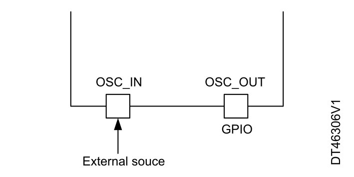
  • HSE user external clock that feeds OSC_IN pin

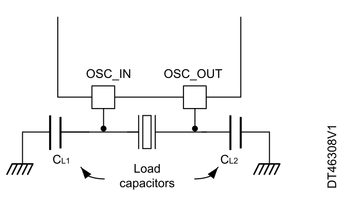
The resonator and the load capacitors must be placed as close as possible to the oscillator pins in order to minimize output distortion and startup stabilization time. The loading capacitance values must be adjusted according to the selected oscillator.

Table 3. HSE/LSE clock sources
Clock sourceHardware configuration
External clock
Crystal/ceramic resonators

CL1 and CL2 values depend on the quartz. Refer to document AN5373_general-info.html#id_14462__entry_phr_xrh_dvb for more details.

External crystal/ceramic resonator (HSE crystal)

The 4 to 50 MHz external oscillator has the advantage of producing a very accurate rate on the main clock. The associated hardware configuration is shown in Table 3 HSE/LSE clock sources. Refer to the electrical characteristics section of the datasheet for more details.

External source (HSE bypass)

In this mode, an external clock source must be provided, with a frequency up to 50 MHz. The external clock signal (square, sinus or triangle) with ~40 to 60 % duty cycle depending on the frequency (refer to the datasheet), must drive the OSC_IN pin while the OSC_OUT pin can be used as a GPIO (see Table 3 HSE/LSE clock sources).

Note:

For details on pin availability, refer to the pinout section of the datasheet. To minimize the consumption, the square signal is recommended.

HSI16 clock

The HSI16 clock signal is generated from an internal 16 MHz RC oscillator. The HSI16 RC oscillator provides a clock source at low cost (no external components). It also has a faster startup time than the HSE crystal oscillator. However, even with calibration, the frequency is less accurate than an external crystal oscillator or ceramic resonator.

The HSI16 clock can be used as a backup clock source (auxiliary clock) if the HSE crystal oscillator fails.

For more details, refer to section Clock security system (CSS) in document AN5373_general-info.html#id_14462__entry_msl_1fh_dvb.

MSI (MSIS and MSIK) clocks

The MSI is made of four internal RC oscillators: MSIRC0 (48 MHz), MSIRC1 (4 MHz), MSIRC2 (3.072 MHz), and MSIRC3 (400 kHz). Each oscillator feeds a prescaler providing a division by 1, 2, 3 or 4.

Two output clocks are generated from these divided oscillators:
  • MSIS that can be selected as system clock
  • MSIK that can be selected by some peripherals as kernel clock

MSIS and MSIK frequency range can be adjusted by software, by using respectively the MSISRANGE [3:0] and MSIKRANGE [3:0] fields in RCC_ICSCR1, with MSIRGSEL = 1. Sixteen frequency ranges are available, generated from the four internal RCs (refer to document AN5373_general-info.html#id_14462__entry_msl_1fh_dvb for more details).

The MSI clock can also be used as a backup clock source (auxiliary clock) if the HSE crystal oscillator fails (refer to section Clock security system (CSS) in document AN5373_general-info.html#id_14462__entry_msl_1fh_dvb).

The MSI oscillator provides a low-cost (no external components) low-power clock source. In addition, when the MSI is used in PLL‑mode with the LSE, it provides a very accurate clock source that can be used by the USB OTG_FS peripheral, and feeds the PLL to run the system at the maximum speed 160 MHz.

Hardware auto calibration with LSE (PLL-mode)

When a 32.768 kHz external oscillator is present in the application, either MSIS or MSIK can be configured in a PLL‑mode. This mode is enabled as follows:
  • for MSIS: by setting the MSIPLLEN bit to 1 in RCC_CR
  • for MSIK: by setting the MSIPLLEN bit to 0 in RCC_CR

In case MSIS and MSIK ranges are generated from the same MSIRC source, the PLL‑mode is applied on both MSIS and MSIK. When configured in PLL‑mode, the MSIS or MSIK automatically calibrates itself thanks to the LSE. This mode is available for all MSI frequency ranges. At 48 MHz, the MSIK in PLL‑mode can be used for the USB OTG_FS peripheral, avoiding the need of an external high‑speed crystal.

For more details on how to measure the MSI frequency variation, refer to section Internal/external clock measurement with TIM15/TIM16/TIM17 in document AN5373_general-info.html#id_14462__entry_msl_1fh_dvb.

Note:

On STM32U5Ax/59x/5Fx/5Gx, the OTG_HS peripheral cannot be clocked by the MSI in PLL‑mode. The HSE crystal must be used.

LSE clock

The LSE crystal is a 32.768 kHz low-speed external crystal or ceramic resonator (see Table 3 HSE/LSE clock sources). It provides a low‑power but highly accurate clock source to the RTC (real-time clock) peripheral for clock/calendar or other timing functions.

The crystal oscillator driving strength can be changed at runtime using the LSEDRV[1:0] bits in RCC_BDCR, to obtain the best compromise between robustness and short startup time on one side, and low-power-consumption on the other side.

External source (LSE bypass)

In this mode, an external clock source must be provided, with a frequency up to 1 MHz. The external clock signal (square, sinus, or triangle) with ~50 % duty cycle, must drive the OSC32_IN pin while the OSC32_OUT pin can be used as GPIO (see Table 3 HSE/LSE clock sources).

Boot mode selection

At startup, a BOOT0 pin, nBOOT0, and NSBOOTADDx[24:0]/SECBOOTADD0[24:0] option bytes are used to select the boot memory address that includes:
  • Boot from any address in user flash memory
  • Boot from system memory (bootloader)
  • Boot from any address in embedded SRAM
  • Boot from root security service (RSS)

The BOOT0 value may come from the PH3-BOOT0 pin or from an option bit depending on the value of a user option bit to free the GPIO pad if needed.

When TrustZone® is disabled by resetting TZEN option bit (TZEN = 0), the boot space is as detailed in the table below.
Table 4. Boot modes when TrustZone® is disabled (TZEN = 0)
nBOOT0

FLASH_

OPTR[27]

BOOT0

pin PH3

nSWBOOT0

FLASH_

OPTR[26]

Boot address option‑byte selectionBoot areaST programmed default value
-01NSBOOTADD0[24:0]Boot address defined by user option bytes NSBOOTADD0[24:0]Flash: 0x0800 0000
-11NSBOOTADD1[24:0]Boot address defined by user option bytes NSBOOTADD1[24:0]Bootloader: 0x0BF9 0000
1-0NSBOOTADD0[24:0]Boot address defined by user option bytes NSBOOTADD0[24:0]Flash: 0x0800 0000
0-0NSBOOTADD1[24:0]Boot address defined by user option bytes NSBOOTADD1[24:0]Bootloader: 0x0BF9 0000

When TrustZone® is enabled by setting the TZEN option bit (TZEN = 1), the boot space must be in a secure area. The SECBOOTADD0[24:0] option bytes are used to select the boot secure memory address. A unique boot entry option can be selected by setting the BOOT_LOCK option bit. All other boot options are ignored.

The table below details the boot modes when the TrustZone® is enabled.
Table 5. Boot modes when TrustZone® is enabled (TZEN = 1)
BOOT_

LOCK

nBOOT0

FLASH_

OPTR[27]

BOOT0

pin

PH3

nSWBOOT0

FLASH_

OPTR[26]

RSS commandBoot address option‑byte selectionBoot areaST programmed default value
0-010SECBOOTADD0[24:0]Secure boot address defined by user option bytes SECBOOTADD0[24:0]Flash: 0x0C00 0000
-110N/ARSSRSS: 0x0FF8 0000
1-00SECBOOTADD0[24:0]Secure boot address defined by user option bytes SECBOOTADD0[24:0]Flash: 0x0C00 0000
0-00N/ARSSRSS: 0x0FF8 0000
---≠ 0N/ARSSRSS: 0x0FF8 0000
1----SECBOOTADD0[24:0]Secure boot address defined by user option bytes SECBOOTADD0[24:0]Flash: 0x0C00 0000