AN5373 · Application noteGetting started with STM32U5 MCU hardware development
Download .pdfOpen in the full document

Power supply schemes

Power supply schemes

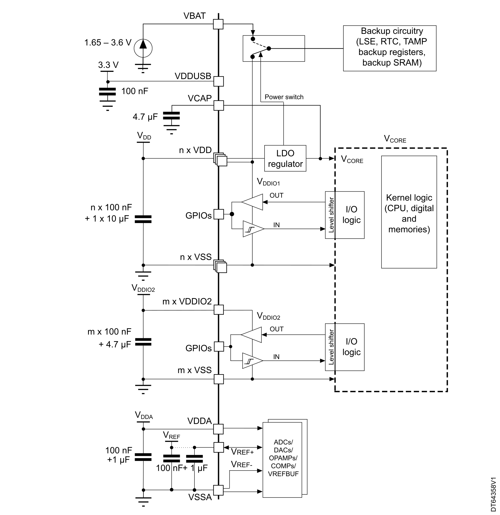
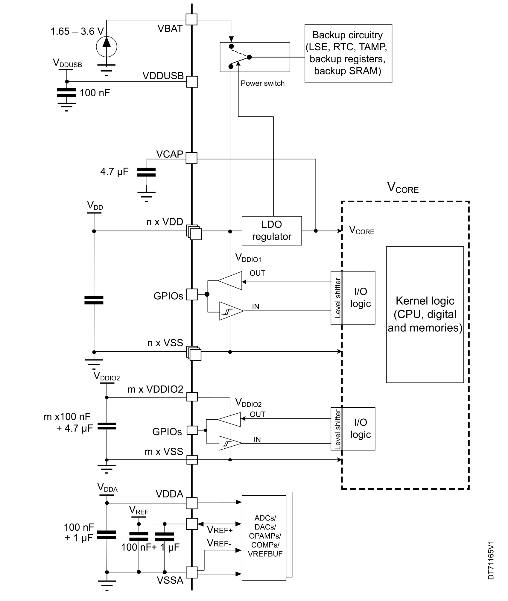
The device is powered by a stabilized VDD power supply as described below:
  • VDD pins must be connected to VDD with external decoupling capacitors: a 10 μF (typical value, 4.7 µF minimum) single tantalum or ceramic capacitor for the package, and a 100 nF ceramic capacitor for each VDD pin.
  • VDD11 pins are present only on packages with SMPS. The SMPS step-down converter requires a 2.2 μH (typical) external ceramic coil connected between VLXSMPS and VDD11 pins. In addition, two 2.2 μF capacitors on VDD11 pins are connected to the VSSSMPS pin.
  • The VCAP pin is present only on standard packages (without SMPS). It requires a 4.7 µF (typical) external decoupling capacitor connected to VSS. If there are two VCAP pins (UFBGA169 package), each VCAP pin must be connected to a 2.2 µF (typical) capacitor (for a total around 4.4 µF).
  • The VDDA pin must be connected to two external decoupling capacitors: 100 nF ceramic and 1 μF tantalum or ceramic.

    Additional precautions can be taken to filter digital noise: VDDA can be connected to VDD through a ferrite bead.

  • The VREF+ pin can be provided by an external voltage reference. In this case, an external 100 nF + 1 μF tantalum or ceramic capacitor must be connected on this pin.

    It can also be provided internally by the VREFBUF. In this case, an external 1 μF (typical) capacitor must be connected on this pin.

  • The VBAT pin can be connected to an external battery to preserve the content of the Backup domain:
    • When VDD is present, the external battery can be charged on VBAT through a 5 kΩ or 1.5 kΩ internal resistor. In this case, the user can insert a capacitor according to the expected discharging time (1 µF is recommended).
    • If no external battery is used in the application, it is recommended to connect the VBAT pin to VDD with a 100 nF external ceramic decoupling capacitor.
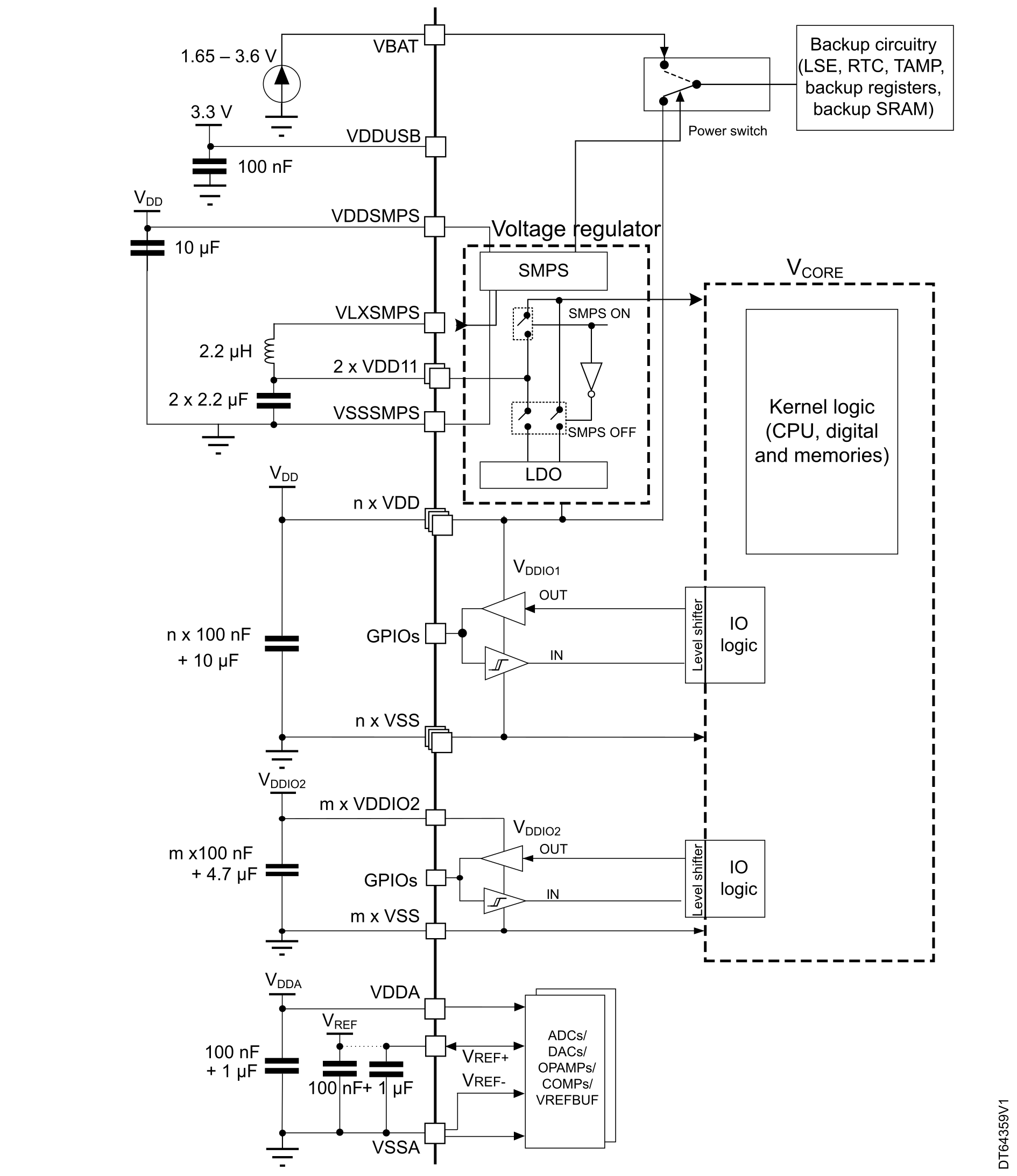
Figure 7. Power supply scheme for U535/545/575/585xxxxQ (with SMPS)
Figure 8. Power supply scheme for STM32U535/545/575/585xx (without SMPS)
CAUTION:

If there are two VCAP pins (UFBGA169 package), each pin must be connected to a 2.2 µF (typical) capacitor (for a total around 4.4 µF).
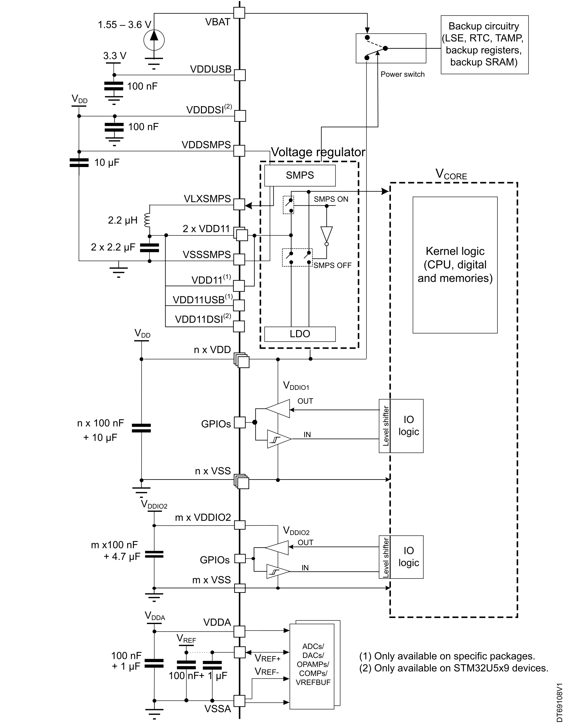
Figure 9. Power supply scheme for STM32U5F/5G/59/5Axxx (with SMPS)
Figure 10. Power supply scheme for STM32U5F/5G/59/5Axxx (without SMPS)
Note:
  • SMPS and LDO regulators provide, in a concurrent way, the VCORE supply depending on application requirements. However, only one of them is active at the same time. When SMPS is active, it feeds the VCORE on the two VDD11 pins provided through the SMPS VLXSMPS output pin. A 2.2 µH coil and a 2.2 μF capacitor on each VDD11 pin are then required. When LDO is active, it provides the VCORE and regulates it using the same decoupling capacitors on VDD11 pins.
  • It is recommended to add a decoupling capacitor of 100 nF near each VDD11 pin/ball, but it is not mandatory.
Power supply isolation

The devices feature a powerful reset system that ensures the main power supply (VDD) has reached a valid operating range before releasing the MCU reset.

This reset system is also in charge of isolating the independent power domains: VDDA, VDDUSB, VDDIO2, and VDD. This reset system is supplied by VDD and is not functional before VDD reaches a minimal voltage (1 V in worse‑case conditions).

To avoid leakage currents between the available supplies and VDD (or ground), VDD must be provided first to the MCU, and then released with tolerance during power down (see Particular conditions during the power-down phase).

General requirements

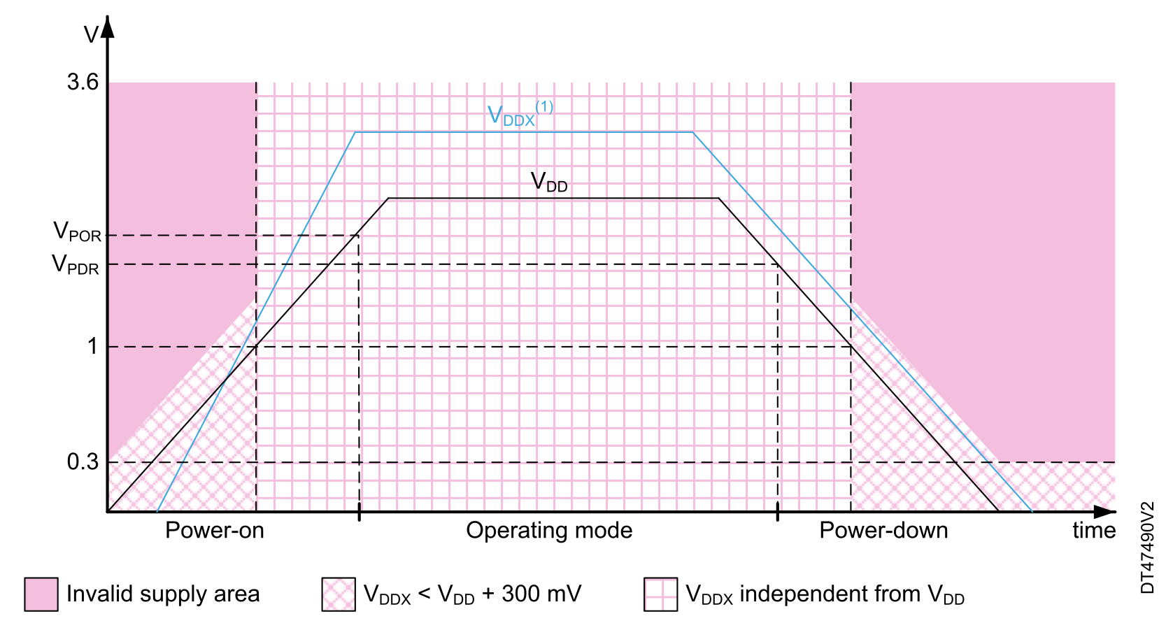
During power-up and power-down phases, the following power sequence requirements must be respected:
  • When VDD is below 1 V, other power supplies (VDDA, VDDIO2, and VDDUSB) must remain below VDD + 300 mV.
  • When VDD is above 1 V, all power supplies are independent.
Figure 11. Power-up/power-down sequence

(1) VDDX refers to any power supply among VDDA, VDDUSB, and VDDIO2.

Note:

VBAT is an independent supply and has no constraint versus VDD. All power supply rails can be tied together.

Particular conditions during the power-down phase

During the power-down phase, VDD can temporarily become lower than other supplies only if the energy provided to the MCU remains below 1 mJ. This allows external decoupling capacitors to be discharged with different time constants during the power-down transient phase (see Figure 11 Power-up/power-down sequence).

VDDX (VDDA, VDDIO2, or VDDUSB) power rails must be switched off before VDD.

Note:

During the power-down transient phase, VDDX can remain temporarily above VDD (see Figure 11 Power-up/power-down sequence).

Example of computation of the energy provided to the MCU during the power-down phase

If the sum of decoupling capacitors on VDDX is 10 μF and VDD drops below 1 V while VDDX is still at 3.3 V, the energy remaining in the decoupling capacitors is:

E = 1 2 ⁢   C × V 2 = 1 2 × 10 − 5 × 3.3 2 = 0.05 ⁢   m J

The energy remaining in the decoupling capacitors is below 1 mJ, so it is acceptable for the MCU to absorb it.

Brownout reset (BOR)

The devices have a brownout reset (BOR) circuitry. The BOR is active in all power modes except Shutdown mode, and cannot be disabled. The BOR monitors the backup domain supply voltage that is VDD when present, VBAT otherwise.

Five BOR thresholds can be selected through option bytes.

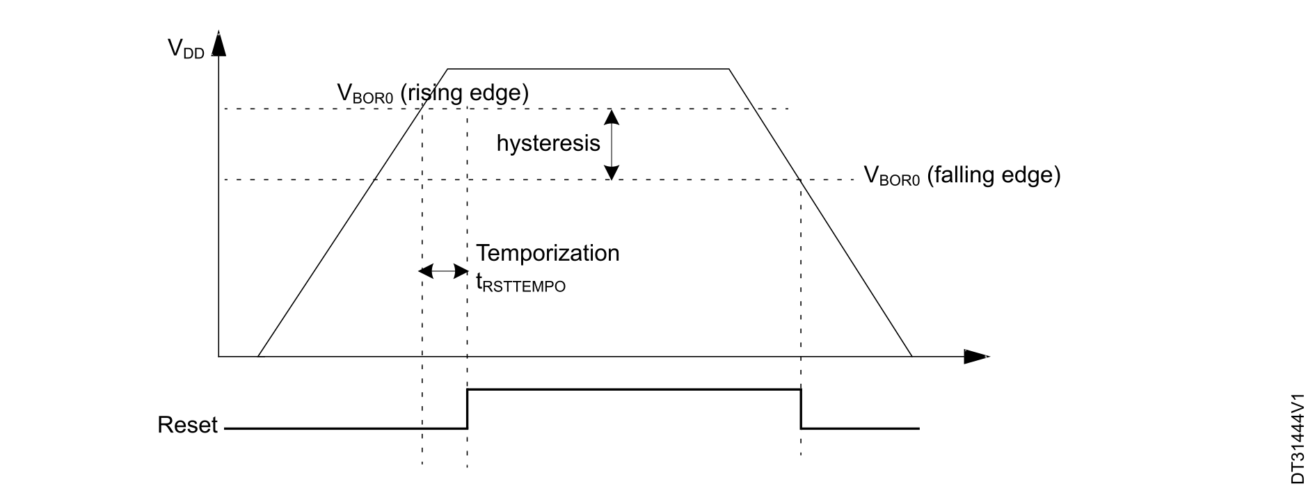
During power-on, the BOR keeps the device under reset until the supply voltage VDD reaches the specified VBORx threshold. When VDD drops below the selected threshold, a device reset is generated. When VDD is above the VBORx upper limit, the device reset is released, and the system can start.

For more details on the brownout reset thresholds, refer to the electrical characteristics section in the datasheet.

Figure 12. Brownout reset waveform


Note:

The reset temporization tRSTTEMPO is present only for the BOR lowest threshold (VBOR0).

System reset

A system reset sets all registers to their reset values except the reset flags in RCC_CSR and the registers in the backup domain.

A system reset is generated when one of the following events occurs (refer to document AN5373_general-info.html#id_14462__entry_msl_1fh_dvb for more details):
  • a low level on the NRST pin (external reset)
  • a window watchdog event (WWDG reset)
  • an independent watchdog event (IWDG reset)
  • a software reset
  • a low-power mode security reset
  • an option-byte loader reset
  • a brownout reset

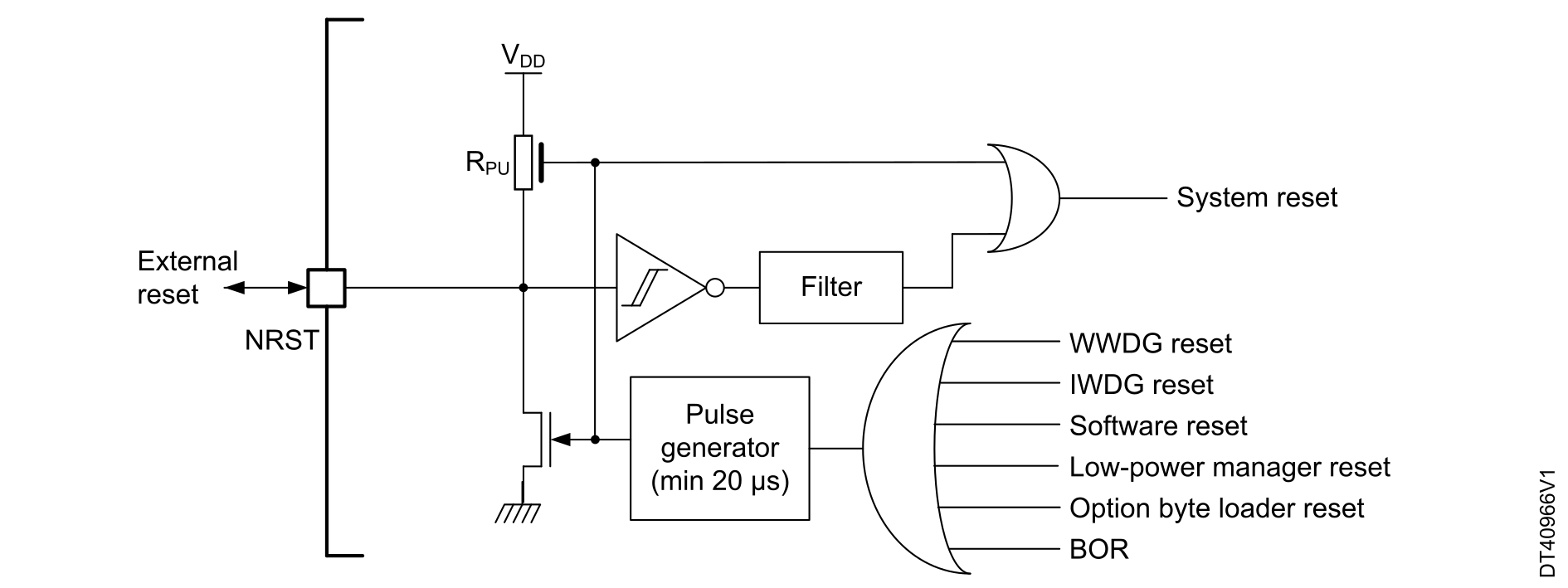
These sources act on the NRST pin that is always kept low during the delay phase. The reset service routine vector is selected via the boot option bytes.

The system reset signal provided to the device is output on the NRST pin. The pulse generator guarantees a minimum reset pulse duration of 20 μs for each internal reset source. In case of an external reset, the reset pulse is generated while the NRST pin is asserted low.

In case of an internal reset, the internal pull-up RPU is deactivated in order to save the power consumption through the pull-up resistor.

Figure 13. Simplified diagram of the reset circuit

Backup domain reset

A backup domain reset is generated when one of the following events occurs:
  • a software reset, triggered by setting the BDRST bit in RCC_BDCR
  • a VDD or VBAT power-on, if both supplies have previously been powered off

A backup domain reset only affects the LSE oscillator, RTC and TAMP, backup registers, the backup SRAM, and RCC_BDCR and PWR_BDCR1.