Digital camera interface pixel pipeline description
Digital camera interface pixel pipeline description
Introduction
This section provides a general overview of the DCMIPP peripheral availability across the STM32H7R7/7S7 and STM32N6x5/6x7 products and gives an easy-to-understand explanation on the DCMIPP integration in the STM32 MCUs architecture.
The DCMIPP provides communication interfaces with high-resolution camera sensor and a pixel processing pipeline to process the acquired pixels into a usable form by the application. Two acquisition interfaces are available: a parallel interface with pins for pixel clock and HSYNC and VSYNC synchronization signals as well as a CSI-2 compliant serial interface to capture pixels from camera sensors. The pixel pipeline applies processing such as decimation, cropping, downsizing, color conversion, gamma correction directly on the received pixels.
It offers higher performance compared to former MCUs by moving from AHB slave (DCMI) to AXI master, increasing data transfer rates from 48 Mbytes to 2800 Mbytes. It supports modern CSI-2 interfaces, accommodating high-resolution sensors.
Additionally, the DCMIPP features a dedicated applicative pipe that spares postprocessing and bandwidth by adapting resolution and pixel format to the application needs. Typically, it downsizes on-the-fly to 1080p-YUV420 for video encoding and to QVGA-RGB for NPU analysis.
The DCMIPP application offers high-speed uncompressed image capture for superior image quality and supports compressed image capture in JPEG format for efficient storage space utilization.
The DCMIPP offers flexible operating modes to support most camera sensors.
It supports both color and monochrome cameras, using various data formats. It is compatible with multiple types of external sensors, including:
Raw Bayer sensors without internal ISP, which output unprocessed raw Bayer pixels
Sensors with an internal ISP, which usually output RGB or YUV pixels
Sensors supporting video compression, which output a bit-stream, such as JPEG or H.264
Sensors with interlaced video, which output their odd and even fields sequentially
Camera module
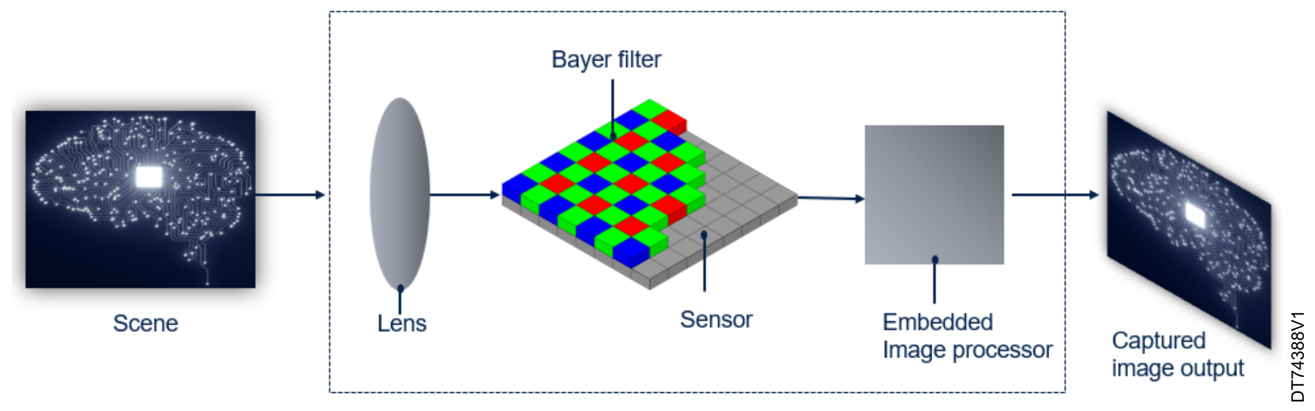
The camera module integrates the following components:
Lens: Focuses light onto the sensor
Bayer matrix and filter: Used to capture color information by filtering the incoming light into red, green, and blue components
Optionally, an image signal processor (ISP): Processes images, converting the raw data from the sensor into a usable format
Data interface such as CSI-2 interface or parallel interface
These elements work together to capture and process images. Digital cameras typically generate YUV, RGB, and raw Bayer output formats. The sensor modules, in particular, generate Raw bayer output format with bit depths that can vary, including 8, 10, 12, and 14 bits. This raw Bayer format preserves the unprocessed data from the sensor, allowing for greater flexibility and precision in postprocessing and image enhancement.Figure 1. Camera module components
Hardware interfaces
The camera module can be interfaced with an MCU using two types of interfaces: parallel and CSI-2.
Parallel interface
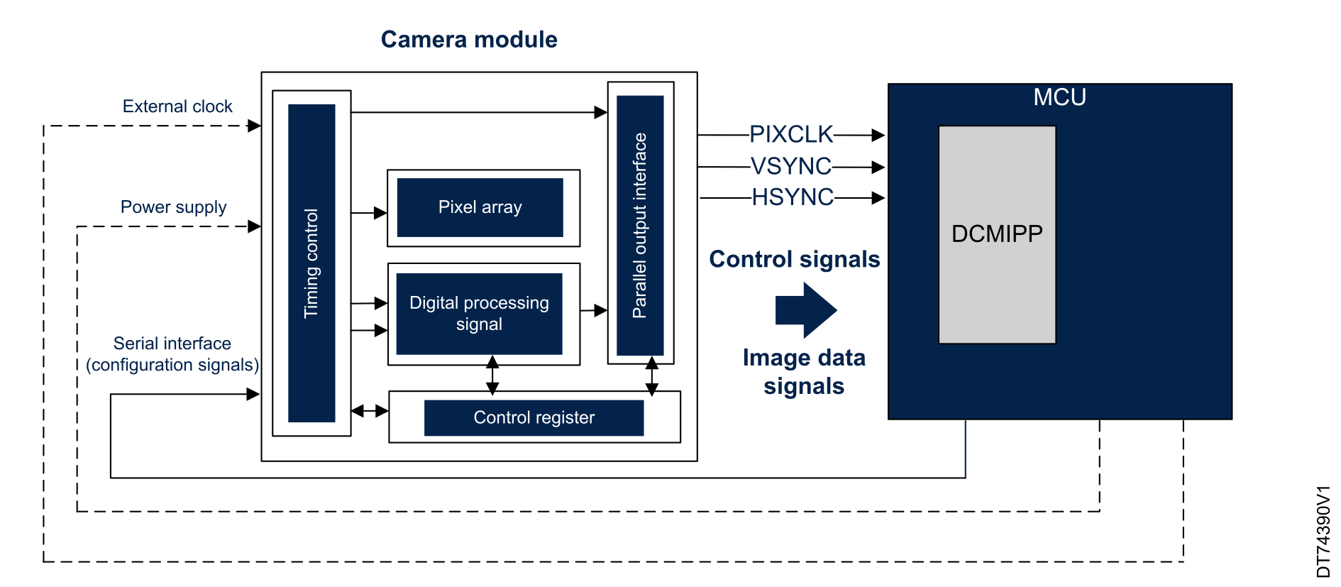
A camera module requires four main types of signals to transmit image data properly: control signals, image data signals, power supply signals, and camera configuration signals.
The interconnection has the following characteristics:
Control signals are used for clock generation and data transfer synchronization
The camera clock must be provided according to the camera specification. The camera also provides two data synchronization signals: HSYNC (for horizontal/line synchronization) and VSYNC (for vertical/frame synchronization).
Image data signals
Each of them transmits a bit of the image data. Their width represents the number of bits to be transferred at each pixel clock. This number depends on both the parallel interface of the camera module and the embedded system interface.
Power supply signals
As any embedded electronic system, the camera module needs to have a power supply. The operating voltage of the camera module is specified in Operating condition section inside the device datasheet reference.
Configuration signals are used for the following:
Configuring image resolution, format, frame rate, contrast, and brightness, over a dedicated I2C interface, even for the parallel interface (to the sensor).
The remaining configuration signal used to select the type of interface could be a combination of a sensor pin configuration and/or a firmware initialization sequence sent to the sensor over I2C.
Note:
Most camera modules are parametrized through an I²C communication bus.
CSI-2 interface
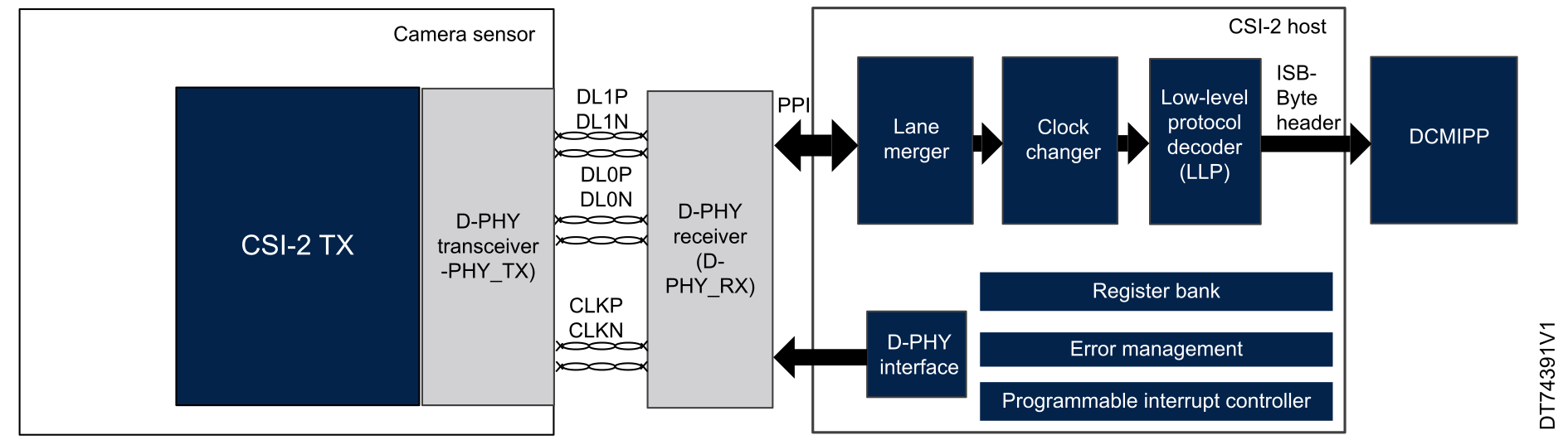
Figure 3. Serial interfacing a camera module with an STM32 MCU
The camera serial interface 2 (CSI-2) is part of a group of communication protocols defined by the MIPI® Alliance.
The MIPI® CSI-2 Host controller is a digital core that implements all protocol functions defined in the MIPI® CSI-2 v1.2 specification.
It provides an interface between the system and the MIPI® D-PHY, enabling communication with CSI-2 compliant cameras. The CSI-2 host connects external serial cameras to the CSI-2 Host controller, using unidirectional slave data lanes and clock lanes to handle data transmission from CSI-2 protocol-based camera devices to subsystems for data processing handled by the DCMIPP.
The STM32N6 interfaces with serial camera modules by incorporating the MIPI® CSI-2 Host controller. This controller, equipped with a D-PHY receiver physical layer, efficiently and cost-effectively extracts and decodes data packets, processing them frame by frame from the CSI-2 device to the host.
The CSI-2 host connects external serial cameras to the CSI-2 Host controller. It is based on unidirectional slave data lanes and clock lanes to handle data transmission from the CSI-2 protocol-based camera devices to subsystems for data processing handled by the DCMIPP.
DCMIPP availability and features across STM32 MCUs
Table 2 DCMIPP capabilities summarizes the STM32 products embedding the DCMIPP. The table also highlights the availability of other hardware resources that facilitates DCMIPP operation. These hardware resources can also be used with the DCMIPP in the same application.
Table 2. DCMIPP capabilities
STM32
Max DCMIPP pixel clock input freq. (MHz)
Max Kernel clock freq. (MHz)
Max DCMIPP Interconnect clock freq. (MHz)
Pipe0 (dump pipe)
Pipe1 (Main Pipe)
Pipe2 (ancillary pipe)
Serial interface (CSI-2)
Parallel interface
STM32H7R3/7S3
STM32H7R7/7S7
120
250
400
Yes
No
No
No
Yes
STM32N6x5
STM32N6x7
120
333
250
Yes
Yes
Yes
Yes
Yes
DCMIPP architecture
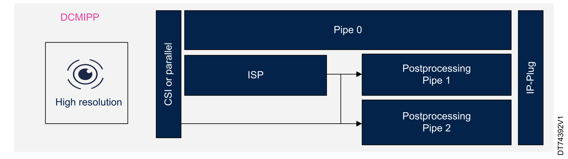
The DCMIPP handles image acquisition and processing through the integrated parallel and abutted CSI-2 interfaces. On the acquisition path, DCMIPP reads input from these interfaces, while on the output path, it writes to memory through the IP-Plug block, acting as an AXI master and using output FIFOs to manage pixel transfers and address memory latency issues. The DCMIPP features include ISP functions in Pipe 1 (shareable with Pipe 2) and differentiated postprocessing pipelines. Pipe 1 and Pipe 2 offer cropping, downsizing, and pixel formatting capabilities.
Figure 4. DCMIPP overview
The DCMIPP offloads the MCU from all image acquisition tasks through up-to-three dedicated camera pipelines, incorporating ISP features for sensor modules such as:
RGB Bayer pattern processing
Bad pixel correction
Decimation
Black level adjustment
Exposure control
Demosaicing
Color conversion
Contrast enhancement
Additionally, it offers robust postprocessing functionalities including:
Cropping
Decimation
Downsizing
Region of interest (ROI) selection
Gamma correction
YUV conversion
Pixel packing
STM32H7R7/7S7 system architecture
The STM32H7R7/7S7 line is a bootflash-based MCU powered by a Cortex®-M7 core running up to 600 MHz, with 64 Kbytes of user bootflash, 620 Kbytes of flexible SRAM, and 32 x 32 Kbytes of cache with Flex ECC.
The STM32H7R7/7S7 devices embed two bus matrices: one 64-bit AXI matrix and one 32-bit AHB matrix. This configuration allows efficient and simultaneous operation of high-speed peripherals and removes bus congestion when several masters are simultaneously active (different masters located in separate bus matrices). Each bus matrix ensures and arbitrates concurrent accesses from multiple masters to multiple slaves. The arbitration uses a round-robin algorithm. The maximum bus matrix frequency is half the maximum CPU frequency.
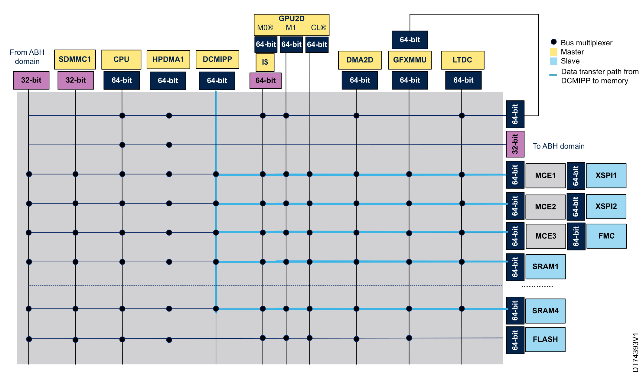
The DCMIPP embeds an AXI bus master to drain all the valid data captured into the pipe from the internal FIFO to the targeted memory.
Figure 5. DCMIPP interconnection and data path on STM32H7R7/7S7
STM32N6x5/6x7 system architecture
The STM32N6x5/6x7 is based on the Arm® Cortex®-M55 running at 800 MHz, the first CPU to introduce Arm Helium vector processing technology, bringing DSP processing capability to a standard CPU.
The STM32N6x5/6x7 is the first STM32 MCU to embed the ST Neural-ART accelerator™, an in-house developed neural processing unit (NPU) engineered for power-efficient edge AI applications. Clocked at 1 GHz and providing up to 600 GOPS, it enables real-time neural network inference for computer vision and audio applications.
A dedicated computer vision pipeline with a MIPI® CSI-2 interface and image signal processing (ISP) ensures compatibility with a wide range of cameras. The STM32N6x5/6x7 also features an H264 hardware encoder and the NeoChrom™ Accelerator for graphics, making it suitable for feature-rich products.
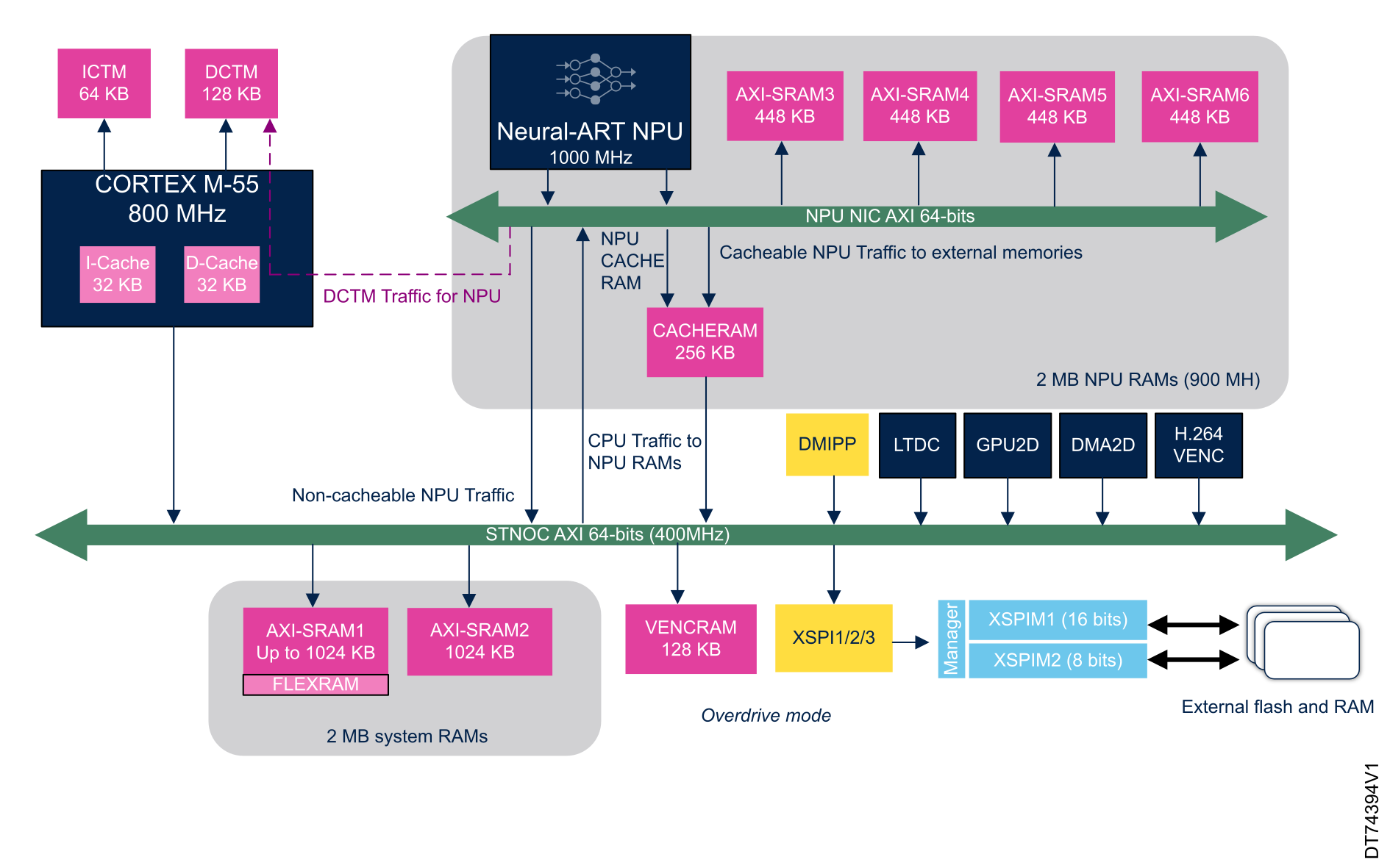
Figure 6 DCMIPP interconnection and data path on STM32N6x7 represents the architecture of the system based on the Cortex-M55 processor and the Neural-ART processing unit (NPU). The Cortex-M55 includes 64 KB ITCM, 128 KB DTCM, and 32 KB I-CACHE, and DCACHE (32 KB) memories. The Neural-ART unit is associated with AXI SRAM3, AXI SRAM4, AXI SRAM5, and AXI SRAM6 memories (448 KB each), as well as a cache memory (CACHERAM of 256 KB) via the NPU NIC AXI 64-bit interface.
The memory system includes up to 1024 KB AXI SRAM1, 1024 KB AXI SRAM2, 128 KB VENC RAM, XSPIM1 (16-bit), and XSPIM2 (8-bit) interfaces for accessing external flash and RAM memories.
The graphical peripherals are composed of:
Digital camera interface pixel pipeline (DCMIPP)
LCD display controller (LTDC)
2D graphics accelerator (GPU2D)
Chrom-ART graphics accelerator (DMA2D)
H.264 video encoder (VENC)
The STNoC AXI 64-bit bus (400 MHz) manages noncacheable NPU traffic and CPU traffic to NPU memories, enabling advanced processing and memory capabilities for applications such as computer vision, signal processing, and machine learning.
Figure 6. DCMIPP interconnection and data path on STM32N6x7