The DCMIPP handles image acquisition and processing through the integrated parallel and abutted CSI-2 interfaces. On the acquisition path, DCMIPP reads input from these interfaces, while on the output path, it writes to memory through the IP-Plug block, acting as an AXI master and using output FIFOs to manage pixel transfers and address memory latency issues. The DCMIPP features include ISP functions in Pipe 1 (shareable with Pipe 2) and differentiated postprocessing pipelines. Pipe 1 and Pipe 2 offer cropping, downsizing, and pixel formatting capabilities.
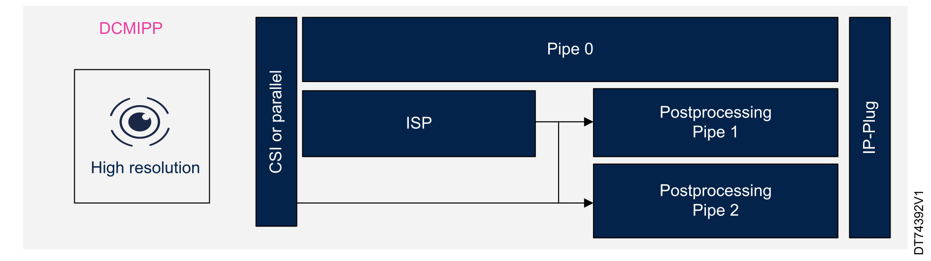
Figure 4. DCMIPP overview
The DCMIPP offloads the MCU from all image acquisition tasks through up-to-three dedicated camera pipelines, incorporating ISP features for sensor modules such as:
RGB Bayer pattern processing
Bad pixel correction
Decimation
Black level adjustment
Exposure control
Demosaicing
Color conversion
Contrast enhancement
Additionally, it offers robust postprocessing functionalities including:
Cropping
Decimation
Downsizing
Region of interest (ROI) selection
Gamma correction
YUV conversion
Pixel packing
STM32H7R7/7S7 system architecture
The STM32H7R7/7S7 line is a bootflash-based MCU powered by a Cortex®-M7 core running up to 600 MHz, with 64 Kbytes of user bootflash, 620 Kbytes of flexible SRAM, and 32 x 32 Kbytes of cache with Flex ECC.
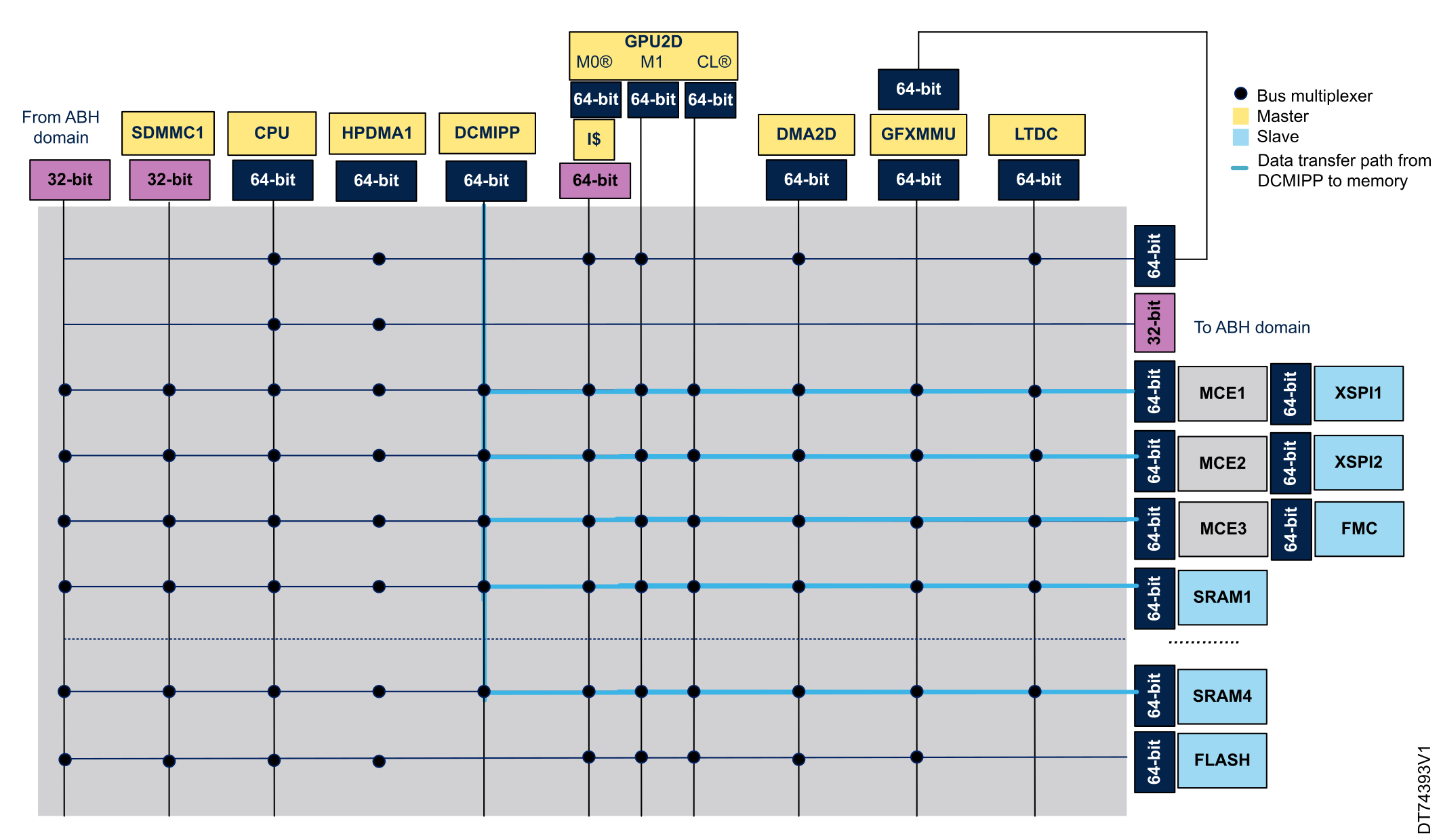
The STM32H7R7/7S7 devices embed two bus matrices: one 64-bit AXI matrix and one 32-bit AHB matrix. This configuration allows efficient and simultaneous operation of high-speed peripherals and removes bus congestion when several masters are simultaneously active (different masters located in separate bus matrices). Each bus matrix ensures and arbitrates concurrent accesses from multiple masters to multiple slaves. The arbitration uses a round-robin algorithm. The maximum bus matrix frequency is half the maximum CPU frequency.
The DCMIPP embeds an AXI bus master to drain all the valid data captured into the pipe from the internal FIFO to the targeted memory.
Figure 5. DCMIPP interconnection and data path on STM32H7R7/7S7
STM32N6x5/6x7 system architecture
The STM32N6x5/6x7 is based on the Arm® Cortex®-M55 running at 800 MHz, the first CPU to introduce Arm Helium vector processing technology, bringing DSP processing capability to a standard CPU.
The STM32N6x5/6x7 is the first STM32 MCU to embed the ST Neural-ART accelerator™, an in-house developed neural processing unit (NPU) engineered for power-efficient edge AI applications. Clocked at 1 GHz and providing up to 600 GOPS, it enables real-time neural network inference for computer vision and audio applications.
A dedicated computer vision pipeline with a MIPI® CSI-2 interface and image signal processing (ISP) ensures compatibility with a wide range of cameras. The STM32N6x5/6x7 also features an H264 hardware encoder and the NeoChrom™ Accelerator for graphics, making it suitable for feature-rich products.
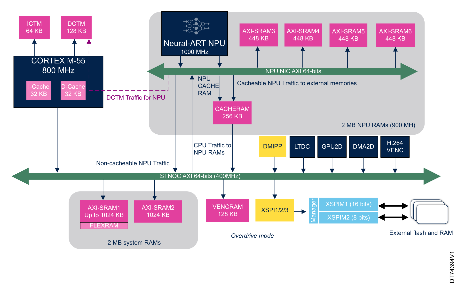
Figure 6 DCMIPP interconnection and data path on STM32N6x7 represents the architecture of the system based on the Cortex-M55 processor and the Neural-ART processing unit (NPU). The Cortex-M55 includes 64 KB ITCM, 128 KB DTCM, and 32 KB I-CACHE, and DCACHE (32 KB) memories. The Neural-ART unit is associated with AXI SRAM3, AXI SRAM4, AXI SRAM5, and AXI SRAM6 memories (448 KB each), as well as a cache memory (CACHERAM of 256 KB) via the NPU NIC AXI 64-bit interface.
The memory system includes up to 1024 KB AXI SRAM1, 1024 KB AXI SRAM2, 128 KB VENC RAM, XSPIM1 (16-bit), and XSPIM2 (8-bit) interfaces for accessing external flash and RAM memories.
The graphical peripherals are composed of:
Digital camera interface pixel pipeline (DCMIPP)
LCD display controller (LTDC)
2D graphics accelerator (GPU2D)
Chrom-ART graphics accelerator (DMA2D)
H.264 video encoder (VENC)
The STNoC AXI 64-bit bus (400 MHz) manages noncacheable NPU traffic and CPU traffic to NPU memories, enabling advanced processing and memory capabilities for applications such as computer vision, signal processing, and machine learning.
Figure 6. DCMIPP interconnection and data path on STM32N6x7
DCMIPP functional description
This section details the DCMIPP and how it handles image data and synchronization signals.
Block diagram
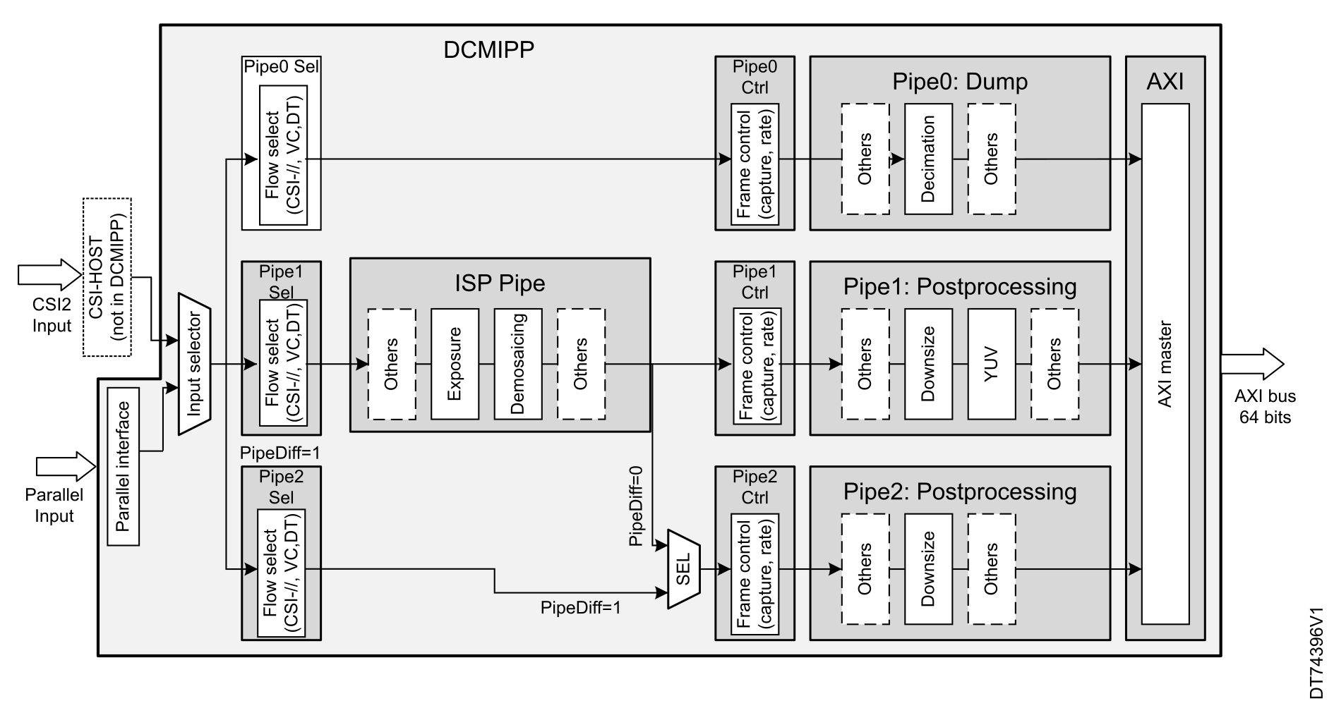
As mentioned in Figure 7 DCMIPP architecture, the DCMIPP receives pixels from either a parallel or CSI interface. Once the pixel data enters, it passes through a flow selector (FLOWSEL) that directs the data to the appropriate processing pipelines.
The architecture features three main pipelines for pixel processing:
Pipe0-Dump serves as a side dump pipe for legacy functions (similar to DCMI), statistics, and raw Bayer data for still images. Depending on the product configuration, it includes stages such as data decimation, reformatting, frame control, and image cropping.
Pipe1-ISP is more complex, it converts raw Bayer into full-resolution RGB. It also adjusts exposure and white balance parameters, with stages such as byte conversion, defective pixel correction, demosaicing, color conversion, and contrast adjustment.
Pipe1-PostProc and Pipe2-PostProc handle postprocessing for different applications, adapting full-resolution RGB to specific needs such as capture rate, cropping, resizing, and color conversion, with the capability to convert to YUV420 for JPEG or H.264 encoding. Both postprocessing pipes include stages such as frame control, cropping, decimation, downsizing, gamma correction, and pixel packing. The Pipe2‑PostProc offers an additional option to sample RGB data before ISP processing. The processed data is then sent to the AXI interface for further use.
Note:
STM32H7R3/7S3 includes only Pipe0-Dump pipeline in the DCMIPP architecture.
Figure 7. DCMIPP architecture
Hardware interfaces
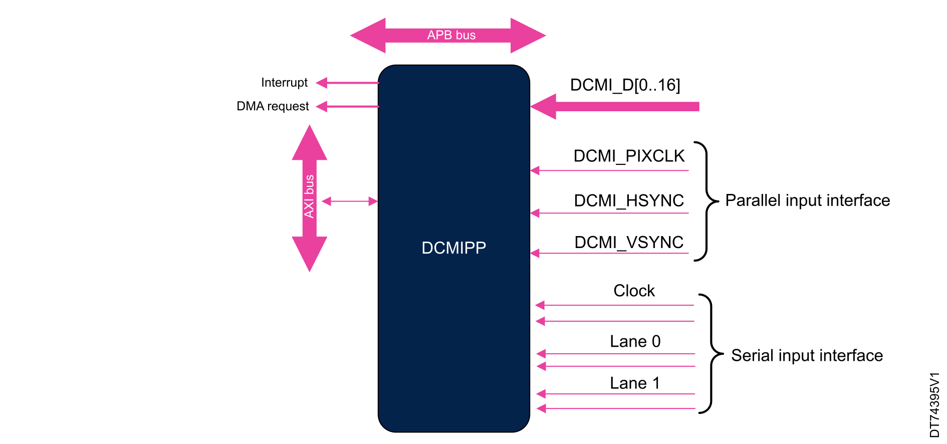
The DCMIPP includes:
Parallel input interface:
Up to 16 data lines (D15-D0)
Pixel clock line DCMIPP _PIXCLK
DCMIPP _HSYNC line (horizontal synchronization)
DCMIPP _VSYNC line (vertical synchronization)
CSI-2 camera serial interface:
Clock lane
Data lanes (Lane 0, Lane 1)
Figure 8. DCMIPP signals
Parallel interface
Hardware synchronization mode
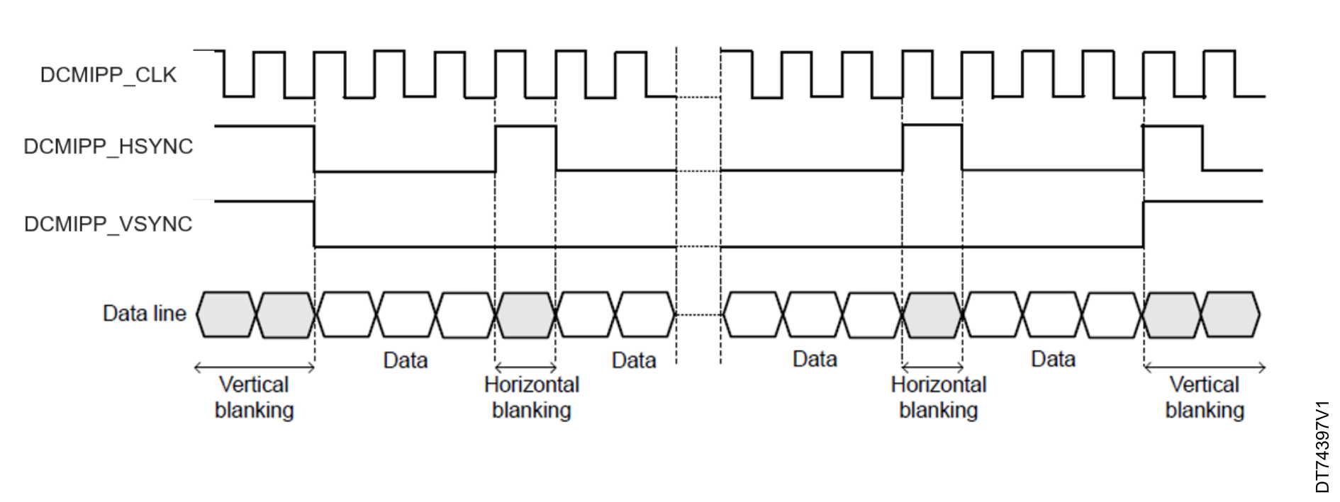
In hardware synchronization mode, the system uses two synchronization signals, DCMIPP_HSYNC and DCMIPP_VSYNC. Depending on the camera module and mode, data can be transmitted during horizontal and vertical synchronization periods. DCMIPP_HSYNC and DCMIPP_VSYNC act as blanking signals, as all data received during DCMIPP_HSYNC and DCMIPP_VSYNC active periods are ignored.
To correctly transfer images in the RAM buffer, data transfer is synchronized with the DCMIPP_HSYNC and DCMIPP_VSYNC signals.
When the hardware synchronization mode is selected and capture is enabled (CPTREQ bit set in DCMIPP_PxFCTCR), data transfer is synchronized with the deassertion of the DCMIPP_VSYNC signal (next start of frame).
Then, the transfer can be continuous, with successive frames transferred by the IP-Plug to either the same buffers, succesive buffers or circular buffers.
Figure 9. Frame structure in hardware synchronization mode
Embedded data synchronization mode
The embedded data synchronization mode is available only with the parallel interface capture mode. In this mode, the data flow is synchronized using embedded 32-bit codes with the values 0x00 and 0xFF, which are no longer used in the data.
There are four types of codes, all with 0xFF0000XY format. The embedded synchronization codes are supported only in 8-bit parallel data capture (in the DCMIPP_PRCR register, the EDM[2:0] bits must be programmed to “000”). For other data widths, the synchronization mode generates unpredictable results.
Note:
Camera modules generate up to eight synchronization codes when in interleaved mode, while the DCMIPP reacts to one single code. Therefore, in an interleaved flow with an embedded synchronization, every other frame is discarded because it is not detected.
Mode 1
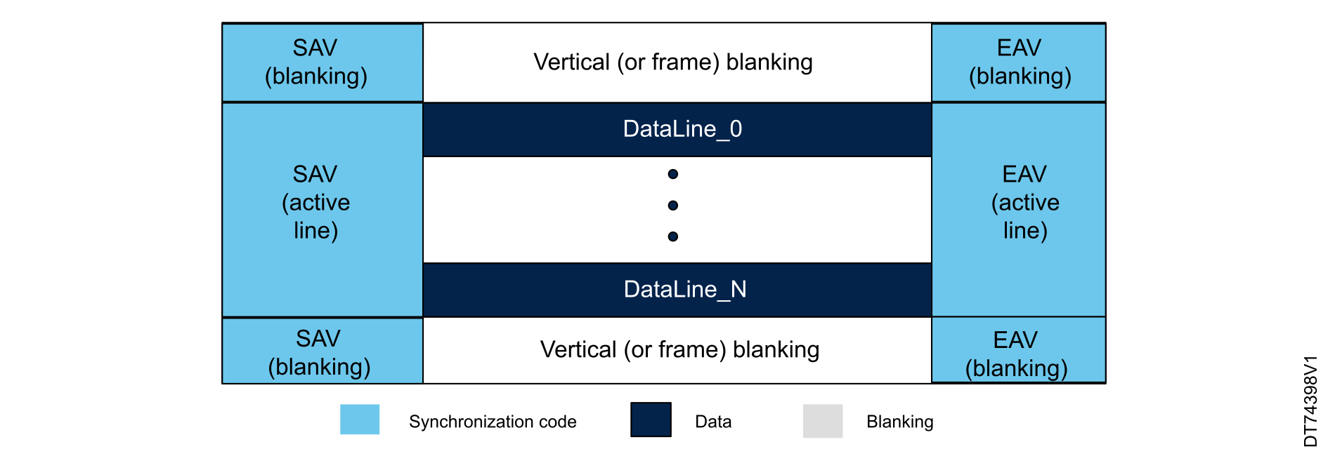
This mode is ITU656 compatible (ITU656 is the digital video protocol of ITU-R BT.656).
The following reference codes indicate a set of four events:
SAV (active line): line-start
EAV (active line): line-end
SAV (blanking): line-start during inter-frame blanking period
EAV (blanking): line-end during inter-frame blanking period
This mode can be supported by programming the following codes:
Figure 10. Frame structure in embedded synchronization mode 1
Mode 2
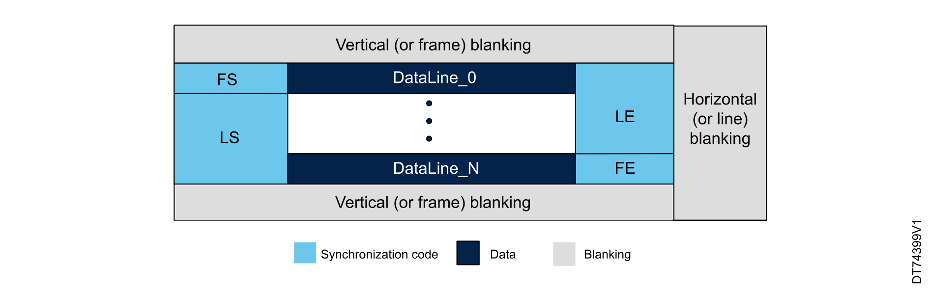
The embedded synchronization codes signal another set of events:
Frame-start (FS)
Frame-end (FE)
Line-start (LS)
Line-end (LE)
A 0xFF value programmed as a frame-end (FE) means that all the unused codes (the possible values of codes other than FS, LS, LE) are interpreted as valid FE codes.
In this mode, once the camera interface has been enabled, the frame capture starts after the first occurrence of an FE code followed by an FS code.
The CSI-2 low-level protocol supports the transport of arbitrary data using both short and long packet formats, with packets transmitted over the physical D-PHY interface. The protocol has the following characteristics:
Transport of arbitrary data
8-bit wordsize
Special packets for frame start, frame end, line start, and line end information
Descriptor for the type, pixel depth, and format of the application-specific payload data
16-bit checksum code for error detection
6-bit error correction code (ECC)
Figure 12. Low-level protocol overview
As illustrated in the figure before, the sequence of the CSI-2 frames begins with an exit from the low-power state (LPS), followed by the start of transmission (SOT) signal, indicating the start of the packet.
Initially, a short packet (SP) is transmitted, followed by the end of transmission (EOT) signal, and a return to low-power state. The sequence then transitions again with SOT to transmit a long packet, which includes a packet header (PH), payload data (DATA), and a packet footer (PF) for error detection, followed by EOT and a return to low-power state. This process repeats for subsequent long packets, ensuring efficient and robust communication.
CSI-2 packet description
The CSI-2 low-level protocol consists of short and long packets, each with a distinct role.
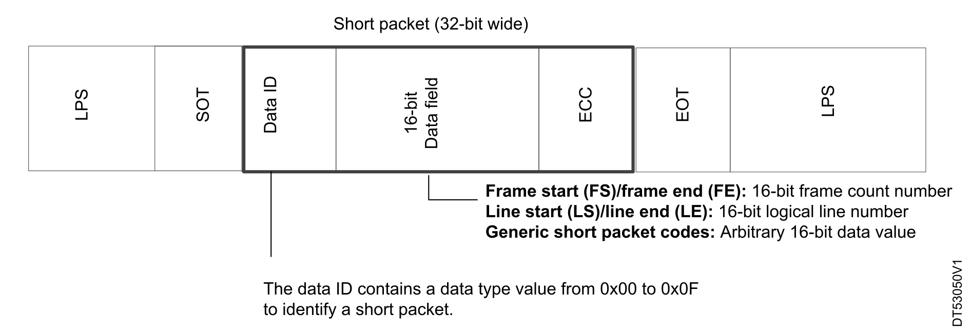
Short packet
The CSI-2 short-packet format for a D-PHY physical layer is shown in the figure below .It is similar to the long packet header, except that the word count field is replaced by a 16-bit data field. The ECC 8-bit code is present to secure headers having potential bit corruption.
Figure 13. CSI-2 short-packet structure based on D-PHY physical layer
Long packet
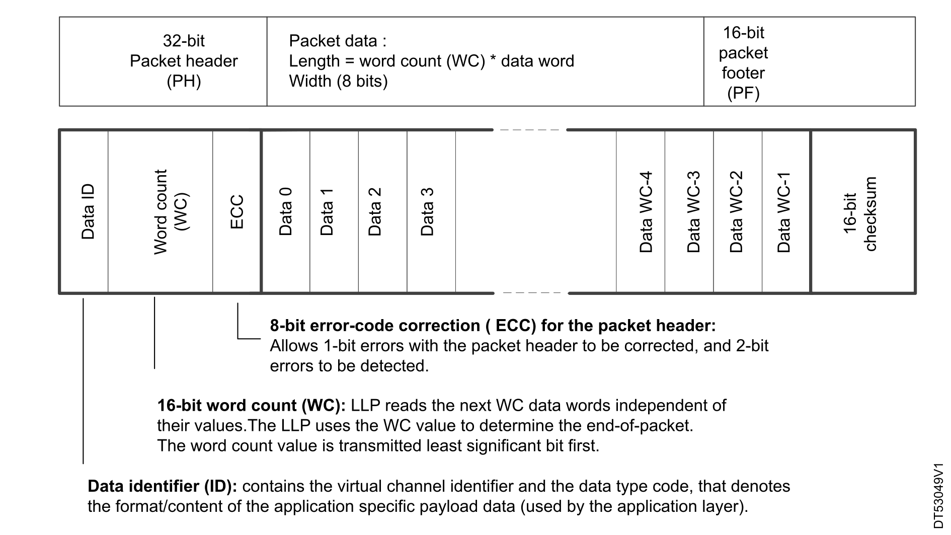
The figure below presents the long packet format. It includes a data ID that consists of a virtual channel number, associated with the data packets, and the corresponding data type.
The word-count field allows the LLP to determine the data-payload width before detecting the packet footer and the EOT. This information is used to detect shorter-than-expected packets, and to trigger a corresponding error
The ECC corrects a single erroneous bit in the packet header in the case of data corruption.
The packet data corresponds to the data payload for a given virtual channel and for an identified data type. To complete the long-packet reception block, a packet footer that contains a 16-bit CRC checksum is received and compared to that which is internally calculated by the LLP, to check the data integrity of the received data payload.
Figure 14. CSI-2 long-packet structure for a D-PHY physical layer
DCMIPP interrupts
The DCMIPP handles the following interrupts for both the parallel interface and all pipes (Pipe 0, Pipe 1, and Pipe 2) :
Parallel interface interrupts
IT_ERR indicates the detection of an error in the embedded synchronization code sequence (only in embedded synchronization mode). This interrupt is indicated by bit 6 in the DCMIPP_PRSR register.
General pipe interrupts:
Specific to Pipe 0
IT_LIMIT: This interrupt is triggered when the received volume is larger than the maximum allowed dump volume. It indicates unexpected behavior in Pipe 0, which usually does not occur if there are no issues.
IT_LINE: This interrupt is for stripe-based operators and is triggered after every 1/2/4/8/16/32/64/128 dumped lines and the last line. It is measured and extracted at the end of the pipe, close to the output to memory.
IT_FRAME: This is a secondary interrupt, serving as a backup for fast software. It is triggered after the last data dump of this pipe and is inactive if no capture has occurred. It is typically used to quickly reconfigure non‑shadow registers (during only vertical blanking) and to trigger the usage of the previously captured frame.
IT_OVR: This interrupt is triggered when there is a data overflow, meaning the memory was too slow compared to the received pixels. This indicates unexpected behavior in Pipe0, which usually does not occur if there are no issues. The recommendation is to skip the impacted frame.
IT_VSYNC: This is the main interrupt, where most software can sit. It is triggered at VSync (mid blanking) and is permanent, even if no dump is active. It is typically used to slowly reconfigure the pipes (at least shadow registers) for the next frame and to trigger the usage of the previously captured frame.
Each pipe has a dedicated interrupt local register that controls the fourth interrupt event (OVR, VSYNC, FRAME, LINE), as indicated in the DCMIPP_P0SR, DCMIPP_P1SR and DCMIPP_P2SR registers for Pipe0, Pipe1, and Pipe2.
DCMIPP events
The DCMIPP contains four events to alert the software to react to certain application situations. These events are linked to the pipeline. The table below mentions these events:
Table 3. DCMIPP events
Pipe
Event
Pipe0
HSYNC
VSYNC
Frame
Line
Pipe1
HSYNC
VSYNC
Frame
Line
Pipe2
HSYNC
VSYNC
Frame
Line
Capture modes
The DCMIPP captures only the frames required by the application optimizing memory access, AXI bus occupation and power consumption. The applicative software may request to get continuous frames from the camera sensor, or only frame in snapshot mode. These two different modes are selected thanks to the bit CPTMODE inside the DCMIPP_PXFSCR register.
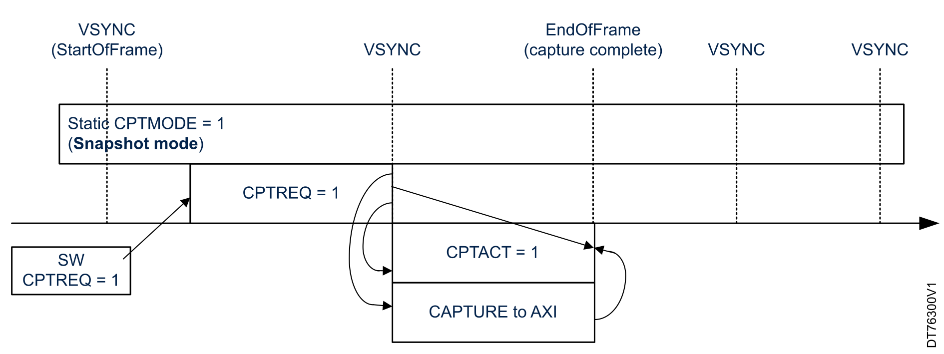
Snapshot mode
In snapshot mode, the software triggers the bit CPTREQ to launch the acquisition from the next start of frame for a single frame only. The bit CPACT remains high only for one frame. It is deasserted at the end of the active frame. At the same time, the bit CPTREQ is cleared by hardware to be ready for future requests, other snapshot acquisitions, or even continuous acquisition after modifying CPTMODE bit in such case.Figure 15. Snapshot capture mode
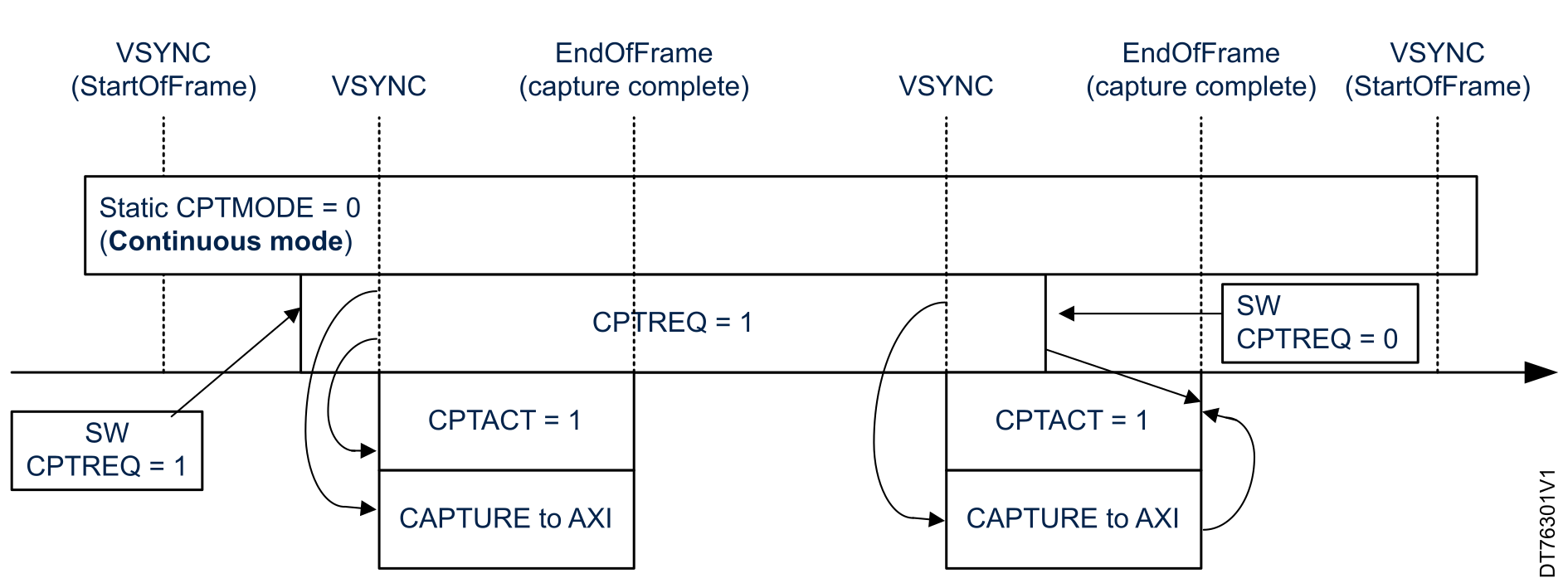
Continuous mode
In continuous mode, the DCMIPP processes the frames continuously. The software needs to arm the bit CPTREQ = 1, and the next VSYNC triggers the data acquisition until the deassertion of this bit. The bit CPTACT remains high, indicating this continuous mode operation.Figure 16. Continuous capture mode