Smart Mobility

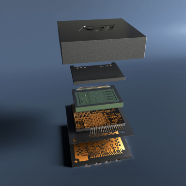
Automotive Power Control
Automotive Power Control
Fully configurable 8-channel pre-driver solution ensures efficient control, safety, and reliable integration in body electronics

Smarter SDV starts here
Smarter SDV starts here
Powering the shift to centralized automotive E/E architectures with smarter distribution, safer control, and higher efficiency

Power & Energy

Multiplier-less PFC
Multiplier-less PFC
Optimized 6-pin transition-mode PFC delivers high efficiency and low THD saves board space and reduces BOM costs.

SLLIMM IPM motor drives
SLLIMM IPM motor drives
Scalable intelligent power modules for home appliance, air conditioning, and industrial motor control

Cloud-connected Autonomous Things
.jpg)
Secure graphics start here.
Secure graphics start here.
Discover STM32H5Ex/Fx MCUs for secure, connected applications with high-performance graphics, large embedded memory, and advanced connectivity.

Next-gen sensing
Next-gen sensing
The IIS3DWB10IS features ISPU 2.0 edge AI processing and rugged reliability for 3-axis industrial predictive maintenance.

Upcoming events
Want to know more about our latest technologies?Come and meet us.
Check out all our upcoming events Check out all our upcoming events


9,000 employees.
Innovation.21,000 patents.
Partnerships.200 active R&D programs.
We have an unwavering commitment to innovation & technology
We innovate to create unique technologies and products that provide our customers the best solutions to address their challenges and opportunities.


29 years of sustainability reporting.
Committed.14 sustainability goals.
Responsible.2027 carbon neutrality commitment.
ST annual integrated report
Our annual integrated report offers an overview of our sustainability performance in 2025 and the goals that guide our actions. We remain committed to respecting people and the planet, and to communicating transparently with our stakeholders.

Newsroom
See all the latest news from ST.
Blog
Read our latest technical articles.
Newsroom
See all the latest news from ST.
STMicroelectronics Reports Q2 2026 Financial Results

STMicroelectronics unveils world’s first ST54M secure mobile chip with post-quantum cryptography for next-generation connected services

STMicroelectronics unveils new compact direct Time-of-Flight 3D LiDAR module bringing high-resolution spatial awareness to compact edge AI systems with industry-leading resolution and performance

STMicroelectronics high-performance vibration sensor with in-sensor AI offers a compelling alternative to piezosensor to fast-growing industrial condition-monitoring market
Blog
Read our latest technical articles.
Rust MEMS drivers: 3 reasons to try and adopt our new sensor drivers written in Rust

Update: 800 V HVDC for AI data centers thanks to 6 kW, 12kW, and 20 kW power delivery boards
Update: New ST54M and PQC, Everything you wanted to know about post-quantum cryptography but were afraid to ask

SLLIMM Compact: 32% smaller while beating efficiency records, this new IPM is shaping the next generation of appliances