AN5020 · Application noteIntroduction to digital camera interface (DCMI) for STM32 MCUs
Download .pdfOpen in the full document

DCMI in a smart architecture

DCMI in a smart architecture

The DCMI is connected to the AHB bus matrix. It is accessed by the DMA to transfer the received image data. The destination of the received data depends on the application.

The smart architecture of STM32 MCUs allows the following:
  • The DMA, as an AHB master, transfers the received data (image number n+1) to the memory, while the CPU processes the previously captured image (image number n).
  • The DMA2D, as an AHB master, is used to transfer or modify the received data (CPU resources are kept for other tasks).
  • The memories throughput and the performance are improved thanks to the multi-layer bus matrix.
STM32F2 system architecture

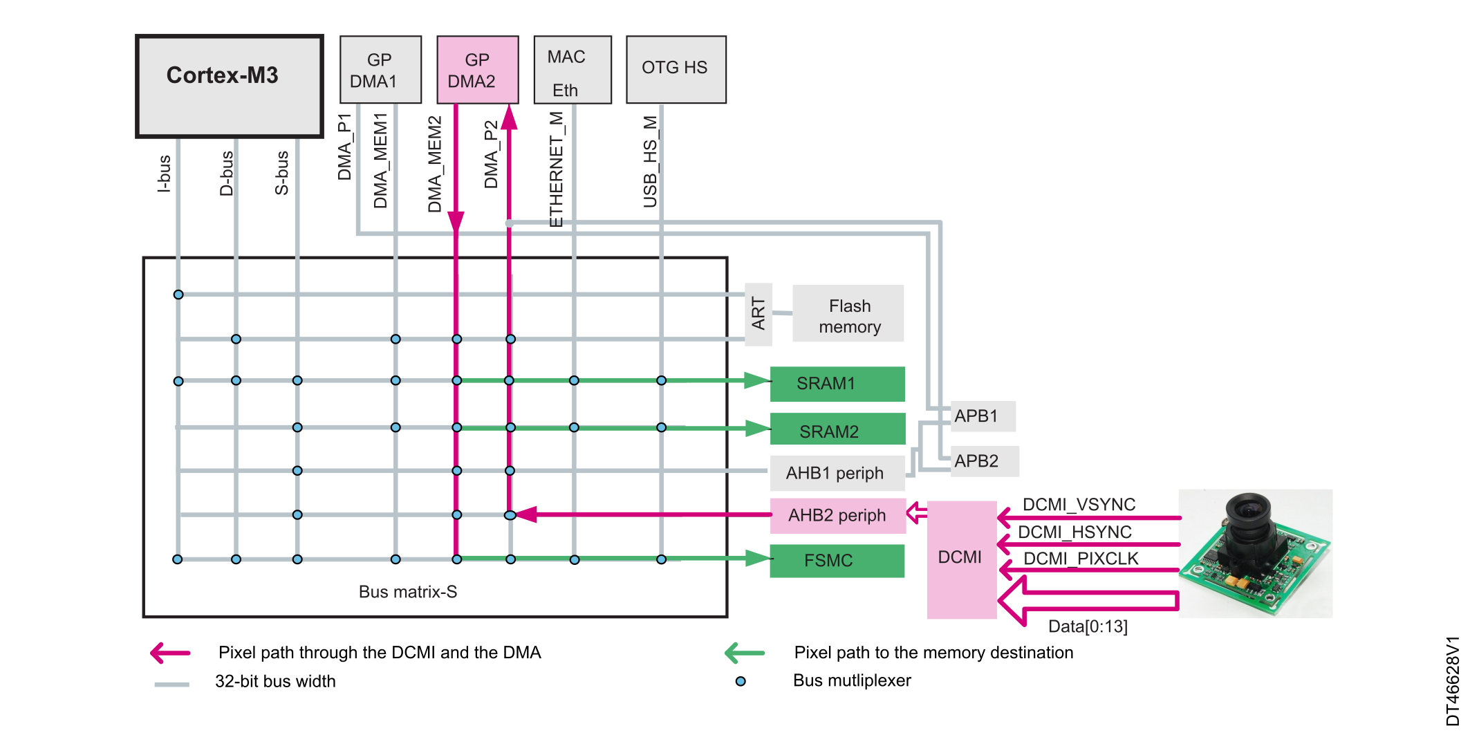
The STM32F2x7 devices are based on a 32-bit multi-layer bus matrix, used to interconnect eight masters and seven slaves. The DCMI is a slave AHB2 peripheral. The DMA2 performs the data transfer from the DCMI to internal SRAMs or external memories through the FSMC.

Figure 6 DCMI slave AHB2 peripheral in the STM32F2x7 shows the DCMI interconnection and the data path in the STM32F2x7 devices.
Figure 6. DCMI slave AHB2 peripheral in the STM32F2x7

STM32F4 system architecture

The STM32F407/417, STM32F427/437, STM32F429/439, STM32F446, and STM32F469/479 line devices are based on a 32-bit multilayer bus matrix, allowing the interconnection between:
  • Ten masters and eight slaves for the STM32F429/439 devices
  • Ten masters and nine slaves for the STM32F469/479 devices
  • Seven masters and seven slaves for the STM32F446 devices
  • Eight masters and seven slaves for the STM32F407/417 devices
  • Eight masters and eight slaves for the STM32F427/437 devices

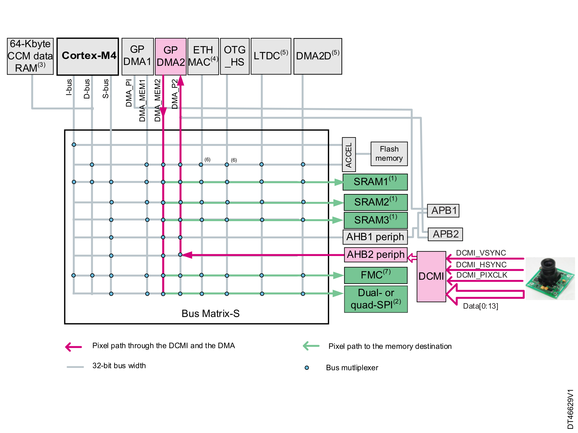
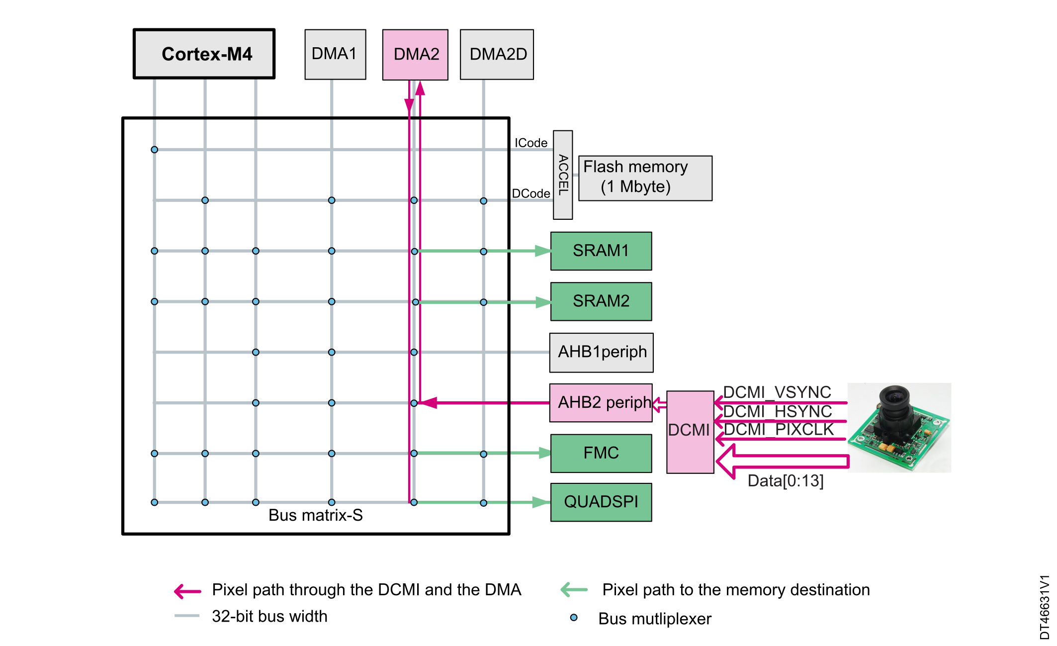
The DCMI is a slave AHB2 peripheral. The DMA2 performs the data transfer from the DCMI to internal SRAMs or external memories through the FMC (FSMC for the STM32F407/417 line) or the QUADSPI.

Figure 7 DCMI slave AHB2 peripheral in the STM32F4 shows the DCMI interconnection and the data path in these devices.
Figure 7. DCMI slave AHB2 peripheral in the STM32F4


Note:
  1. See the table below for details on the SRAMs.
  2. The dual- or quad-SPI interface is available only in the STM32F469/479 and STM32F446 devices.
  3. The 64-Kbyte CCM data RAM is not available in the STM32F446xx devices.
  4. The Ethernet MAC interface is not available in the STM32F446xx devices.
  5. The LTDC and DMA2D are only available in the STM32F429/439 and STM32F469/479 devices.
  6. In the STM32F407/417 devices, there is no interconnection between:
    • The Ethernet master and the DCode bus of the flash memory
    • The USB master and the DCode bus of the flash memory

    In the STM32F446 devices, there is no interconnection between the USB master and the DCode bus of the flash memory.

  7. It is FMSC for the STM32F407/417 devices.
Table 3. SRAM availability in the STM32F4 series
STM32 lineSRAM1 (Kbytes)SRAM2 (Kbytes)SRAM3 (Kbytes)
STM32F407/41711216N/A
STM32F427/437, STM32F429/43964
STM32F446N/A
STM32F469/47916032128

STM32F7 system architecture

The STM32F7x5, STM32F7x6, STM32F7x7, STM32F7x8, and STM32F7x9 line devices, and the STM32F750 devices in the STM32F7x0 value line are based on a 32-bit multilayer bus matrix, allowing the interconnection between:
  • Twelve masters and eight slaves for the STM32F7x6, STM32F7x7, STM32F7x8, STM32F7x9, and STM32F750 devices
  • Eleven masters and eight slaves for the STM32F7x5 devices

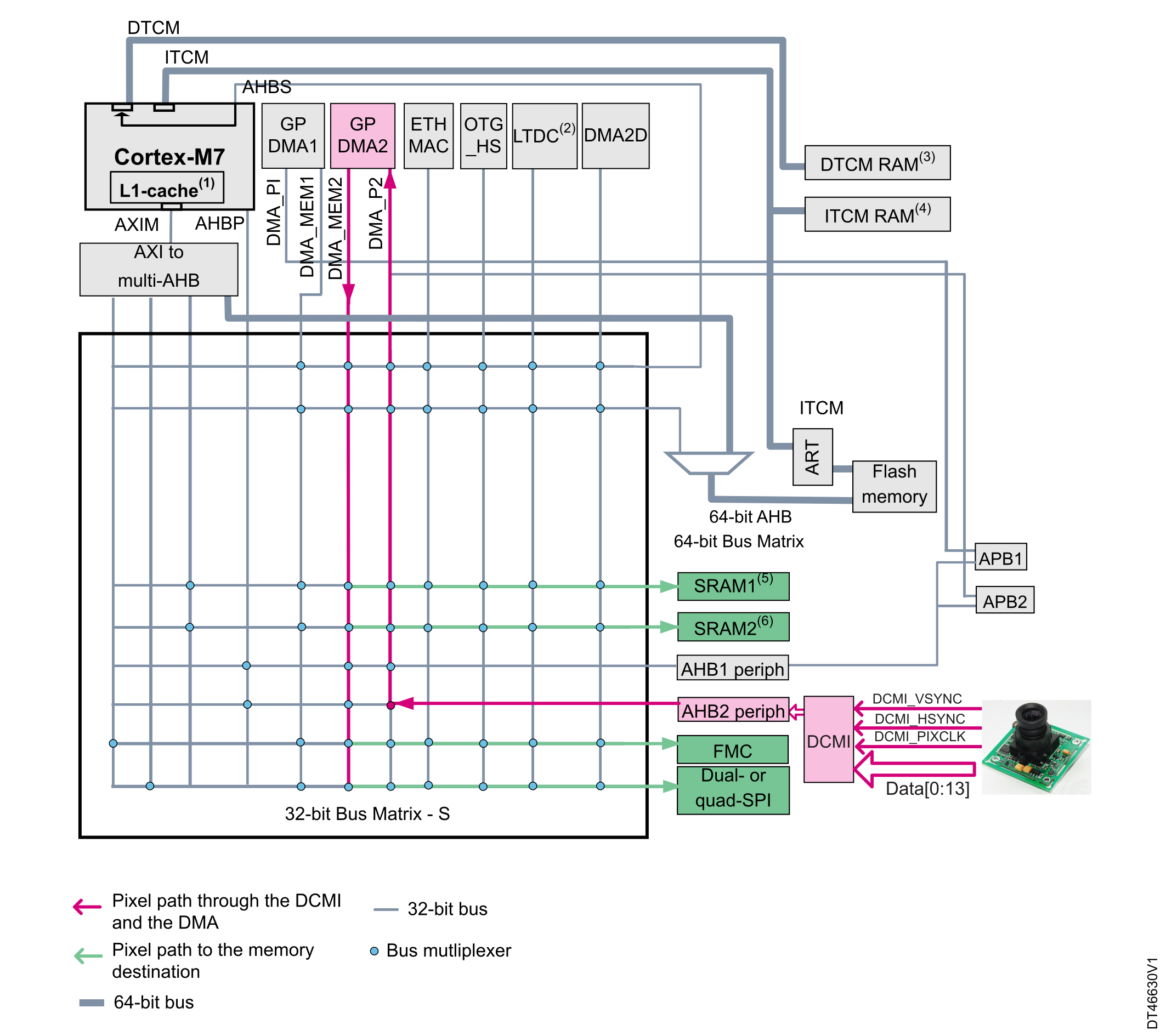
The DCMI is a slave AHB2 peripheral. The DMA2 performs the data transfer from the DCMI to internal SRAM or external memories through the FMC or the QUADSPI.

Figure 8 DCMI slave AHB2 peripheral in the STM32F7 shows the DCMI interconnection and the data path in these devices.
Figure 8. DCMI slave AHB2 peripheral in the STM32F7


Note:
  1. The I/D cache size is:
    • 4 Kbytes for the STM32F7x5/F7x6 and STM32F750 devices
    • 16 Kbytes for the STM32F7x7/F7x8/F7x9 devices
  2. The LTDC is only available in the STM32F7x6/F7x7/F7x8/F7x9 and STM32F750 devices.
  3. The DTCM RAM size is:
    • 64 Kbytes for the STM32F7x5/F7x6 and STM32F750 devices
    • 128 Kbytes for the STM32F7x7/F7x8/F7x9 devices
  4. The ITCM RAM size is 16 Kbytes for the STM32F7x6/F7x7/F7x8/F7x9 and STM32F750 devices.
  5. The SRAM1 size is:
    • 240 Kbytes for the STM32F7x5/F7x6 and STM32F750 devices
    • 368 Kbytes for the STM32F7x7/F7x8/F7x9 devices
  6. The SRAM2 size is 16 Kbytes for the STM32F7x6/F7x7/F7x8/F7x9 and STM32F750 devices.

STM32H7 system architecture

The STM32H723/733, STM32H743/753, STM32H7A3/B3, STM32H747/757, STM32H745/755, STM32H742, STM32H725/735, STM32H750, and STM32H730 line devices are based on an AXI bus matrix, two AHB bus matrices, and bus bridges allowing the interconnection between:
  • 23 masters and 18 slaves for the STM32H745/755 and STM32H747/757 devices
  • 18 masters and 18 slaves for the STM32H723/733, STM32H725/735, STM32H753, and STM32H730 devices
  • 19 masters and 18 slaves for the STM32H742 and STM32H743 devices
  • 19 masters and 20 slaves for the STM32H7A3/B3 devices
  • 19 masters and 17 slaves for the STM32H750 Value line devices
STM32H7x3, STM32H742, STM32H725/735, STM32H730, and STM32H750 devices

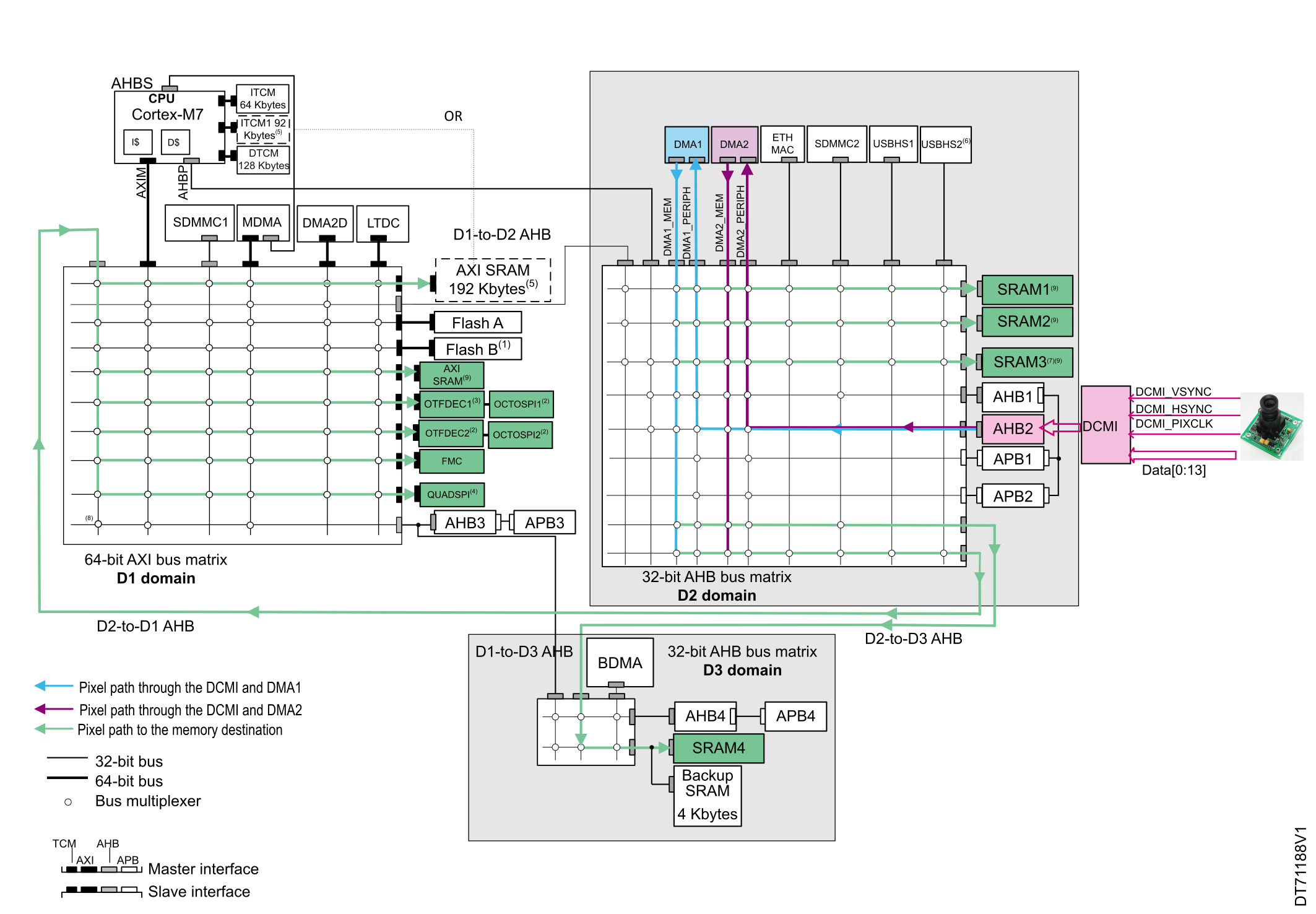
The DCMI is a slave AHB2 peripheral. The DMA1 and DMA2 perform the data transfer from the DCMI to internal SRAMs or external memories through the FMC, the QUADSPI, or the OCTOSPI.

The DMA1 and DMA2 are located in the D2 domain. They are able to access the slaves in the D1 and D3 domains. As a result, the DMA1 and DMA2 can transfer the data received by the DCMI (located in D2) to memories located in the D1 or D3 domains.

Figure 9 DCMI slave AHB2 peripheral in the STM32H723/733, STM32H743/753, STM32H742, STM32H725/735, STM32H730, and STM32H750 devices shows the DCMI interconnection and the data path in these devices.
Figure 9. DCMI slave AHB2 peripheral in the STM32H723/733, STM32H743/753, STM32H742, STM32H725/735, STM32H730, and STM32H750 devices


Note:

1. Flash B is not available in the STM32H723/733, STM32H725/735, STM32H730, and STM32H750 devices.

2. OCTOSPI1 and 2 are not available in the STM32H743/753, STM32H742, and STM32H750 devices.

3. OTFDEC1 and 2 are only available in the STM32H723/733, STM32H725/735, and STM32H730 devices.

4. The QUADSPI is only available in the STM32H743/753, STM32H742, and STM32H750 devices.

5. The 192-Kbyte AXI SRAM and the 92-Kbyte ITCM are only available in the STM32H723/733, STM32H725/735, and STM32H730 devices.

6. The USBHS2 is only available in the STM32H743/753, STM32H742, and STM32H750 devices.

7. The SRAM3 is only available in the STM32H743/753, STM32H74,2 and STM32H750 devices.

8. There is no connection between the APB3 and the D2 domain in the STM32H723/733, STM32H725/735, STM32H730, and STM32H750 devices.

9. See Table 4 SRAM availability in the STM32H723/733, STM32H743/753, STM32H742, STM32H725/735, STM32H730, and STM32H750 devices for more details on the SRAM1, SRAM2, SRAM3 and the AXI SRAM.

Table 4. SRAM availability in the STM32H723/733, STM32H743/753, STM32H742, STM32H725/735, STM32H730, and STM32H750 devices
STM32 lineSRAM1 (Kbytes)SRAM2 (Kbytes)SRAM3 (Kbytes)AXI SRAM (Kbytes)
STM32H723/7331616X128
STM32H725/7351616X128
STM32H7301616X128
STM32H743/75312812832512
STM32H74212812832512
STM32H75012812832512
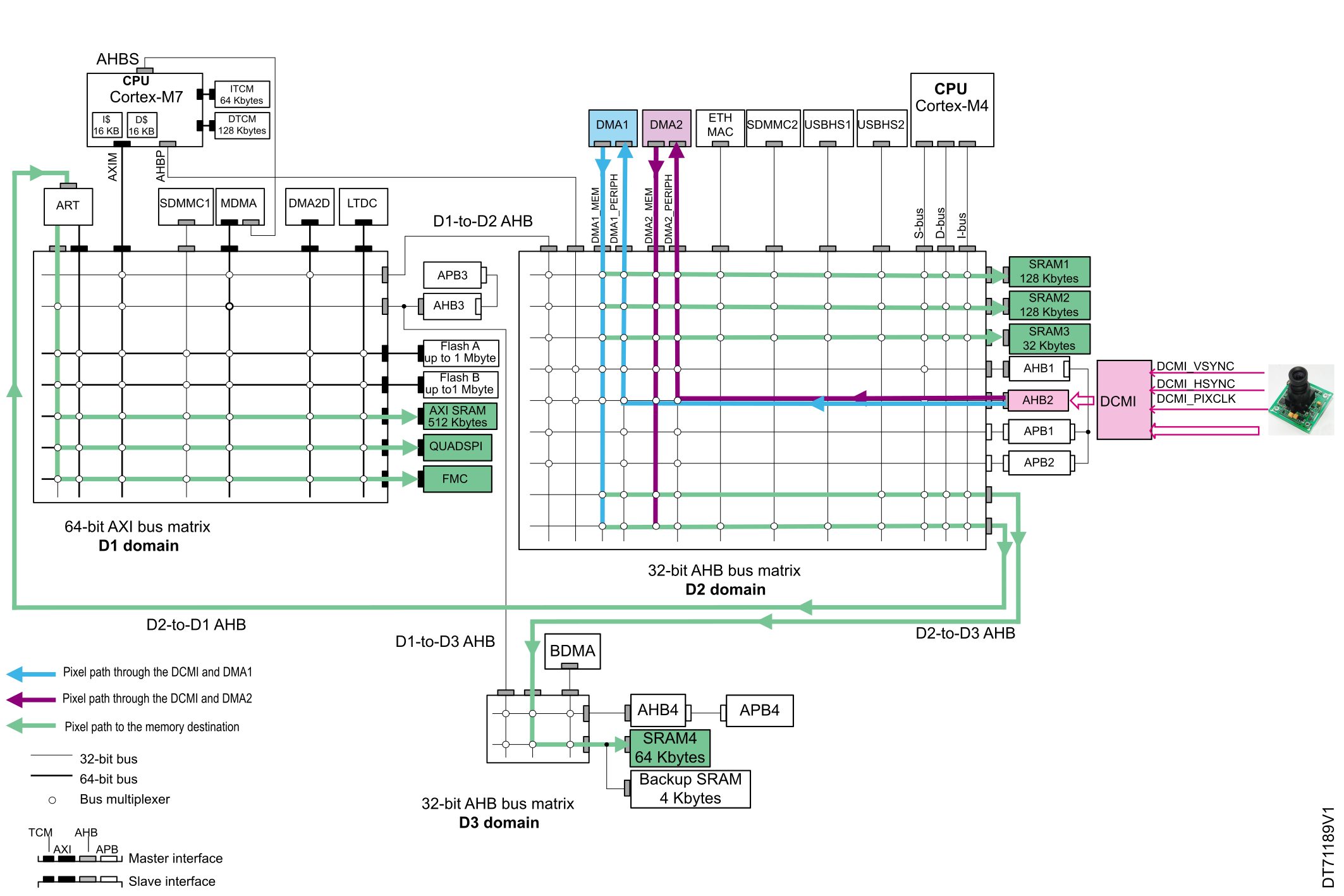
STM32H745/755 and STM32H747/757 devices
The DMA1 and DMA2 are in the D2 domain. They are able to access slaves in the D1 and D3 domains. As a result, the DMA1 and DMA2 can transfer the data received by the DCMI (located in D2) to memories located in the D1 or D3 domains. Figure 10 DCMI slave AHB2 peripheral in the STM32H745/755 and STM32H747/757 devices shows the DCMI interconnection and the data path in these devices.
Figure 10. DCMI slave AHB2 peripheral in the STM32H745/755 and STM32H747/757 devices


STM32H7A3/7B3 devices

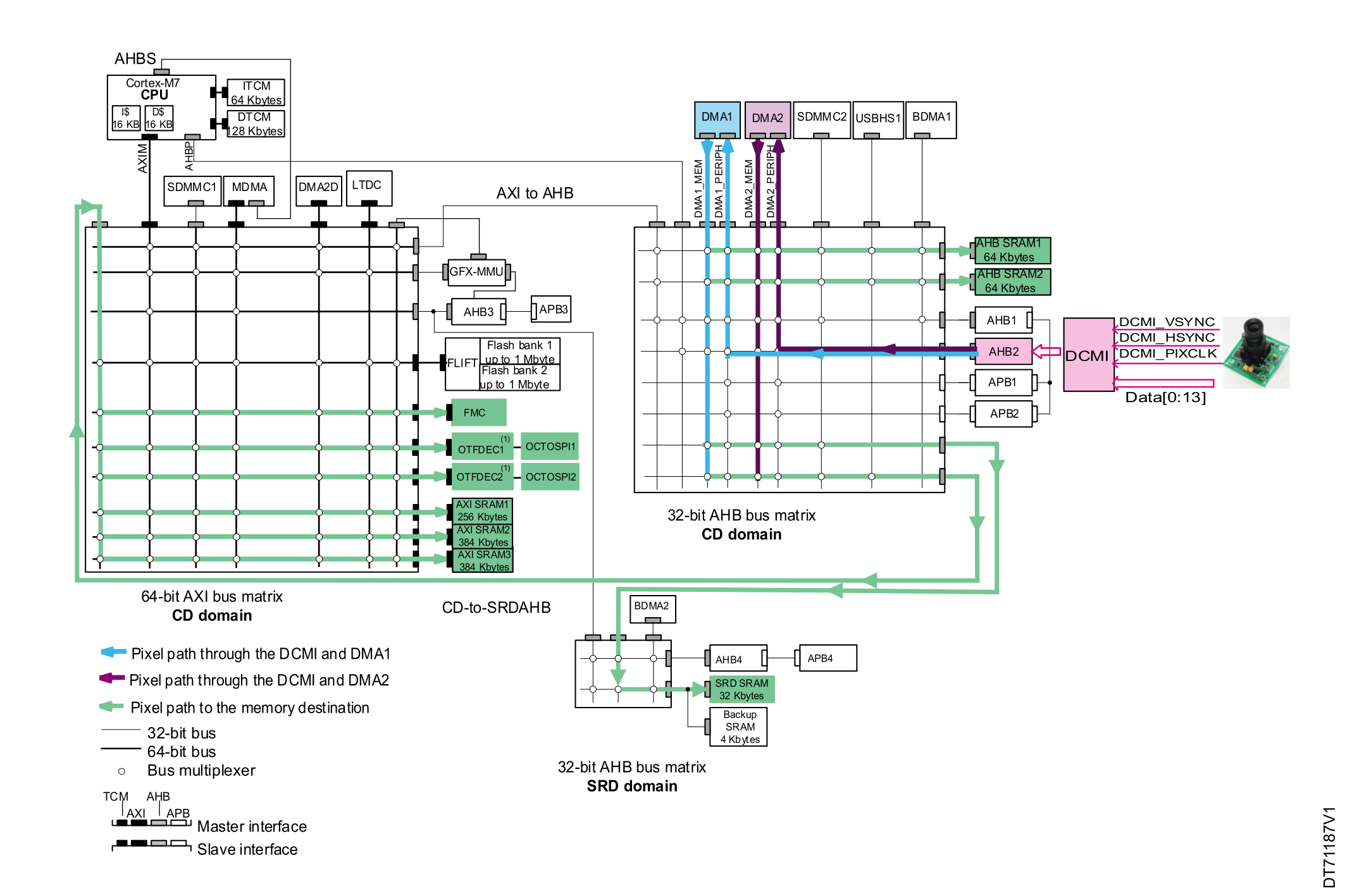
The DMA1 and DMA2 are in the CD domain. They are able to access slaves in the CD and SRD domains. As a result, the DMA1 and DMA2 can transfer the data received by the DCMI (located in the CD domain) to memories located in the CD or SRD domain. Figure 11 DCMI slave AHB2 peripheral in the STM32H7A3/B3 shows the DCMI interconnection and the data path in these devices.

Figure 11. DCMI slave AHB2 peripheral in the STM32H7A3/B3


Note:

OTFDEC1/2 are only available in the STM32H7B3 devices.

STM32L4 system architecture

The STM32L496xx and STM32L4A6xx devices are based on a 32-bit multilayer bus matrix, allowing the interconnection between six masters and eight slaves.

The DCMI is a slave AHB2 peripheral. The DMA2 performs the data transfer from the DCMI to internal SRAMs or external memories through the FMC or QUADSPI.

The DMA has only one port (not like STM32F2/F4/F7 and STM32H7 devices where the peripheral port is separated from the memory port), but it supports circular-buffer management, peripheral-to-memory, memory‑to‑peripheral, and peripheral-to-peripheral transfers.

Figure 12 DCMI slave AHB2 peripheral in STM32L496/4A6 shows the DCMI interconnection and the data path in these devices.
Figure 12. DCMI slave AHB2 peripheral in STM32L496/4A6


STM32L4+ system architecture

The STM32L4R9/S9, STM32L4R7/S7, STM32L4R5/S5, and STM32L4P5/Q5 line devices are based on a 32-bit multilayer bus matrix, allowing the interconnection between:
  • 9 masters and 10 slaves for the STM32L4P5/Q5 devices
  • 9 masters and 11 slaves for the STM32L4R5/S5, STM32L4R7/S7, and STM32L4R9/S9 devices

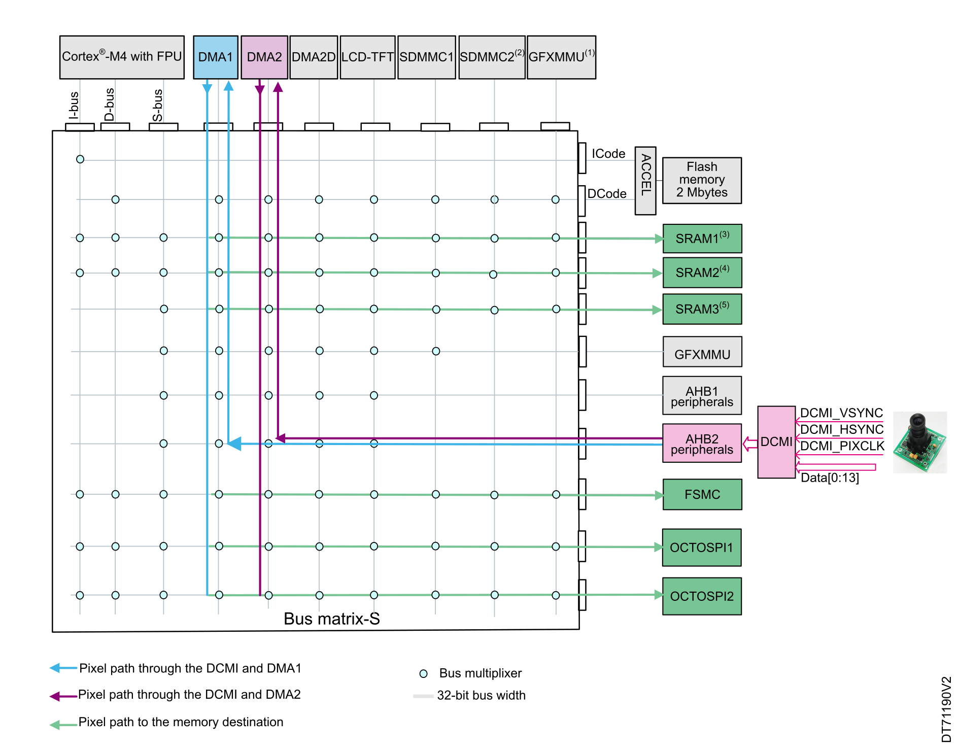
The DCMI is a slave AHB2 peripheral. The DMA1 and DMA2 perform the data transfer from the DCMI to internal SRAMs or external memories through the FSMC or OCTOSPI.

The DMA has only one port. It is different from the STM32F2/F4/F7 and STM32H7 devices where the peripheral port is separated from the memory port. However, it supports circular-buffer management, memory-to-memory, peripheral‑to‑memory, memory-to-peripheral, and peripheral-to-peripheral transfers.

Figure 13 DCMI slave AHB2 peripheral in the STM32L4+ shows the DCMI interconnection and the data path in these devices.

Figure 13. DCMI slave AHB2 peripheral in the STM32L4+


Note:
  1. The GFXMMU is only available in the STM32L4R5/4R7/4R9/4S5/4S7/4S9 devices.
  2. The SDMMC1 is only available in the STM32L4P5/4Q5 devices.
  3. The SRAM1 size is:
    • 128 Kbytes for the STM32L4P5/4Q5 devices
    • 192 Kbytes for the STM32L4R5/4R7/4R9/4S5/4S7/4S9 devices.
  4. The SRAM2 size is 64 Kbytes for the STM32L4P5/4Q5/R5/4R7/4R9/4S5/4S7/4S9 devices.
  5. The SRAM3 size is:
    • 128 Kbytes for the STM32L4P5/4Q5 devices
    • 384 Kbytes for the STM32L4R5/4R7/4R9/4S5/4S7/4S9 devices

STM32U5 system architecture

The STM32U5 devices are based on a 32-bit multilayer AHB bus matrix, enabling the interconnection between:
  • 16 masters and 13 slaves in the STM32U595/5A5, STM32U599/5A9, STM32U5F7/5G7, and STM32U5F9/5G9 devices
  • 11 masters and 10 slaves in the STM32U575/585 devices
  • 9 masters and 7 slaves in the STM32U535/545 devices

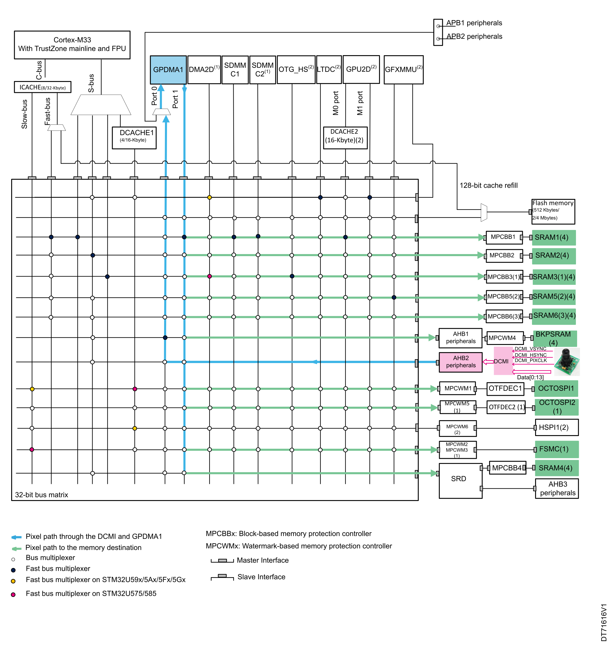
The DCMI is a slave AHB2 peripheral.

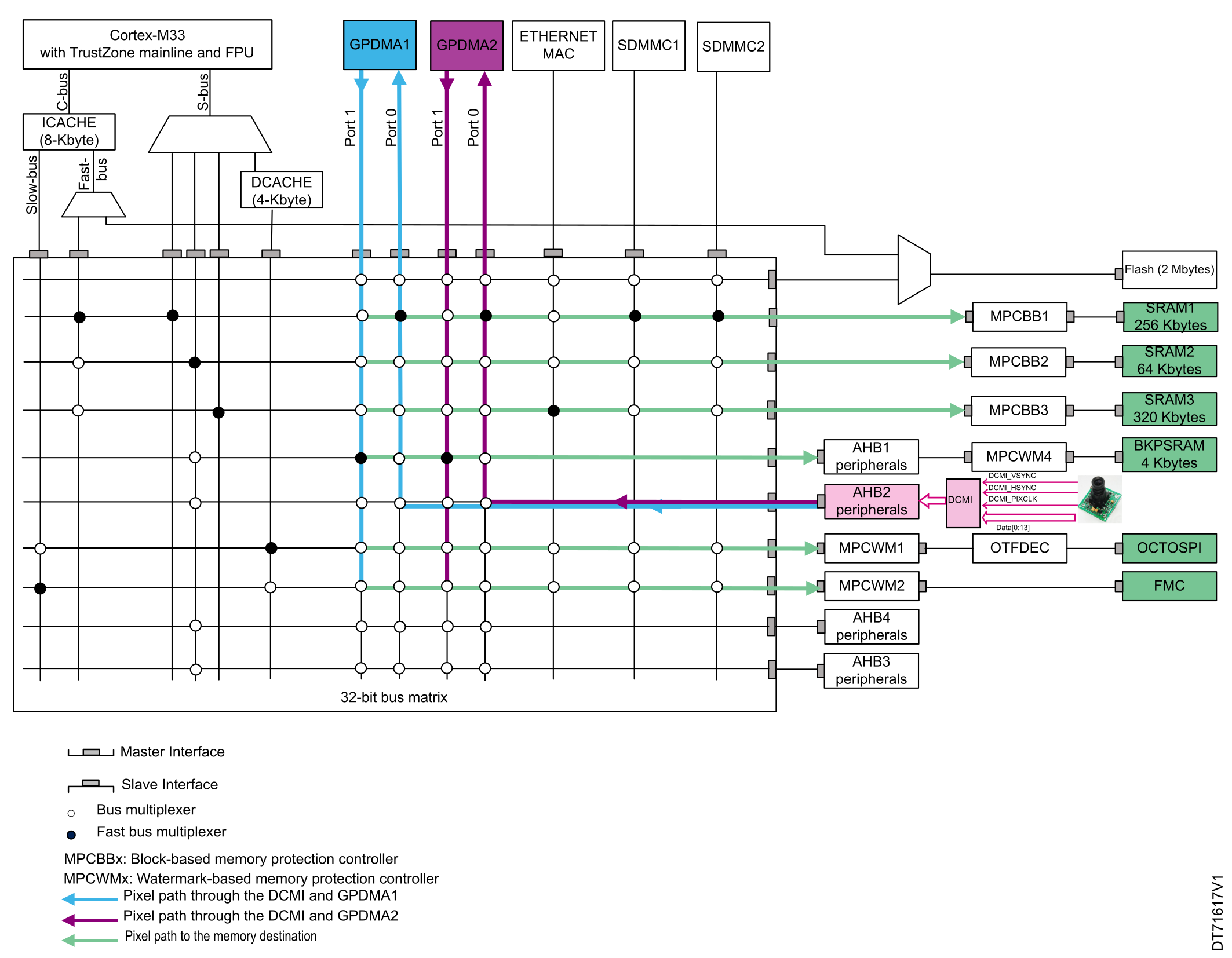
The GPDMA1 performs the data transfer from the DCMI to internal SRAMs or external memories through the FSMC, OCTOSPI, or HSPI.

Figure 14 DCMI slave AHB2 peripheral in the STM32U5 devices shows the DCMI interconnection and the data path in these devices.

Figure 14. DCMI slave AHB2 peripheral in the STM32U5 devices


Note:
  1. This peripheral is not present in the STM32U535/545.
  2. This peripheral is not present in the STM32U535/545/575/585.
  3. This peripheral is present only in the STM32U5F7/5G7, STM32U5F9/5G9.
  4. See Table 5 SRAM availability in the STM32U5 devices for more details on the SRAM1/2/3/4/5/6 and the BKPSRAM
Table 5. SRAM availability in the STM32U5 devices
STM32 linesSRAM1 (Kbytes)SRAM2 (Kbytes)SRAM3 (Kbytes)SRAM4 (Kbytes)SRAM5 (Kbytes)SRAM6 (Kbytes)BKSRAM (Kbytes)
STM32U535/54519264x16xx2
STM32U575/5851926451216xx2
STM32U595/5A5 STM32U599/5A97686483216832x2
STM32U5F7/5G7 STM32U5F9/5G976864832168325122

STM32H5 system architecture

The STM32H562 and STM32H563/573 devices are based on a 32-bit multilayer AHB bus matrix, enabling the interconnection between 13 masters and 10 slaves.

The DCMI is a slave AHB2 peripheral.

The GPDMA1 performs the data transfer from the DCMI to internal SRAMs or external memories through the FMC or OCTOSPI.

Figure 15 DCMI slave AHB2 peripheral for the STM32H562 and STM32H563/573 shows the DCMI interconnection and the data path in these devices.

Figure 15. DCMI slave AHB2 peripheral for the STM32H562 and STM32H563/573


STM32N6 system architecture

The STM32N6 devices are based on a 32-bit multilayer AHB bus matrix, enabling the interconnection between 28 masters and 29 slaves.

The DCMI is a slave AHB5 peripheral. The GPDMA performs the data transfer from the DCMI to internal SRAM or external memories through the FMC or the XSPI.