AN5020 · Application noteIntroduction to digital camera interface (DCMI) for STM32 MCUs
Download .pdfOpen in the full document

DCMI configuration

Capture mode selection

The user can capture an image or a video by selecting one of the following modes:
  • The continuous grab mode to capture frames (images) continuously
  • The snapshot mode to capture a single frame

The received data in snapshot or continuous grab mode is transferred to the memory frame buffer by the DMA. The buffer location and mode (linear or circular buffer) are controlled through the system DMA.

Data format selection

The DCMI allows the reception of compressed data (JPEG) or many uncompressed data formats (such as monochrome, RGB, or YCbCr). For more details, refer to Data formats and storage.

Image resolution and size

The DCMI allows the reception of a wide range of resolutions (low, medium, high) and image sizes, since the image size depends on the image resolution and data format. The DMA ensures the transfer and the placement of the received images in the memory frame buffer.

Optionally, the user can configure the byte, line, and frame select mode to modify the image resolution and size, and in some cases, the data format (see Image resizing (resolution modification)). The user can also configure and enable the crop feature to select a rectangular window from the received image (see Crop feature).

Note:

The DCMI configuration registers must be programmed correctly before enabling the ENABLE bit in DCMI_CR. The DMA controller and all DCMI configuration registers must be programmed correctly before enabling the CAPTURE bit in DCMI_CR.

DMA configuration

The DMA configuration is a crucial step to ensure the success of the application.

As mentioned in DCMI in a smart architecture, the DMA2 ensures the transfer from the DCMI to the memory (internal SRAM or external SRAM/SDRAM) for all STM32 devices embedding the DCMI.

For the STM32H7 and SMT32L4+ devices, the DMA1 can also access the AHB2 peripherals and ensures the transfer of the received data from the DCMI to the memory frame buffer.

For the STM32U5 and STM32N647/657 devices, the GPDMA1 ensures the transfer from the DCMI to the memory.

For the STM32H5 devices, the GPDMA1 and the GPDMA2 ensure the transfer from the DCMI to the memory.

DMA configuration for DCMI-to-memory transfers

The transfer direction must be peripheral-to-memory by configuring:
  • DIR bits in DMA_SxCR for the STM32F2, STM32F4, STM32F7, and STM32H7 devices
  • DIR bits in DMA_CCRx for the STM32L4x6 and STM32L4+ devices
  • SWREQ = 0 and REQSEL[6:0] in GPDMA_CxTR2 for the STM32U5 and STM32H5
The source address (DCMI data register address) must be written:
  • In DMA_SxPAR for the STM32F2, STM32F4, STM32F7, and STM32H7 devices
  • In DMA_CPARx for the STM32L4x6 and STM32L4+ devices
  • In GPDMA_CxSAR for the STM32U5, STM32H5, and STM32N647/657 devices
The destination address (frame buffer address in internal SRAM or external SRAM/SDRAM) must be written:
  • In DMA_SxMAR for the STM32F2, STM32F4, STM32F7, and STM32H7 devices
  • In DMA_CMARx for the STM32L4x6 and STM32L4+ devices
  • In GPDMA_CxDAR for the STM32U5, STM32H5, and STM32N647/657 devices

To ensure the data transfer from the DCMI data register, the DMA waits for the request to be generated from the DCMI. The relevant stream and channel must be configured. For more details, refer to DCMI channel and stream configuration.

Since a DMA request is generated each time the DCMI data register is filled, the data transferred from the DCMI must have a 32-bit width. Data is transferred:
  • To the DMA2 (or the DMA1 for the STM32H7 and STM32L4+ devices) for all STM32 except for the STM32U5, STM32H5, and STM32N647/657
  • To the GPDMA1 for the STM32U5, STM32H5, and STM32N647/657 devices
  • To the GPDMA2 for the STM32H5 devices
The peripheral data width must be 32-bit words. It is programmed:
  • By PSIZE bits in DMA_SxCR for the STM32F2, STM32F4, STM32F7, and STM32H7 devices
  • By PSIZE bits in DMA_CCRx register for the STM32L4x6 and STM32L4+ devices
  • By DDW_LOG2 and DBL_1 in GPDMA_CxTR1 for the STM32U5, STM32H5, and STM32N647/657 devices
The DMA is the flow controller: the number of 32-bit data words to be transferred is software programmable from 1 to 65535 (see DMA_SxNDTR/DMA_CNDTRx/GPDMA_CxBR1 register for more details):
  • In DMA_SxNDTR for the STM32F2, STM32F4, STM32F7, and STM32H7 devices
  • In DMA_CNDTRx for the STM32L4x6 and STM32L4+ devices
  • In GPDMA_CxBr1 for the STM32U5, STM32H5, and STM32N647/657 devices
The DMA operates in one of the following modes:
  • Direct mode: each word received from the DCMI is transferred to the memory frame buffer.
  • FIFO mode: the DMA uses its internal FIFO to ensure burst transfers (more than one word from the DMA FIFO to the memory destination).

For more details on the DMA internal FIFO, refer to FIFO and burst transfer configuration.
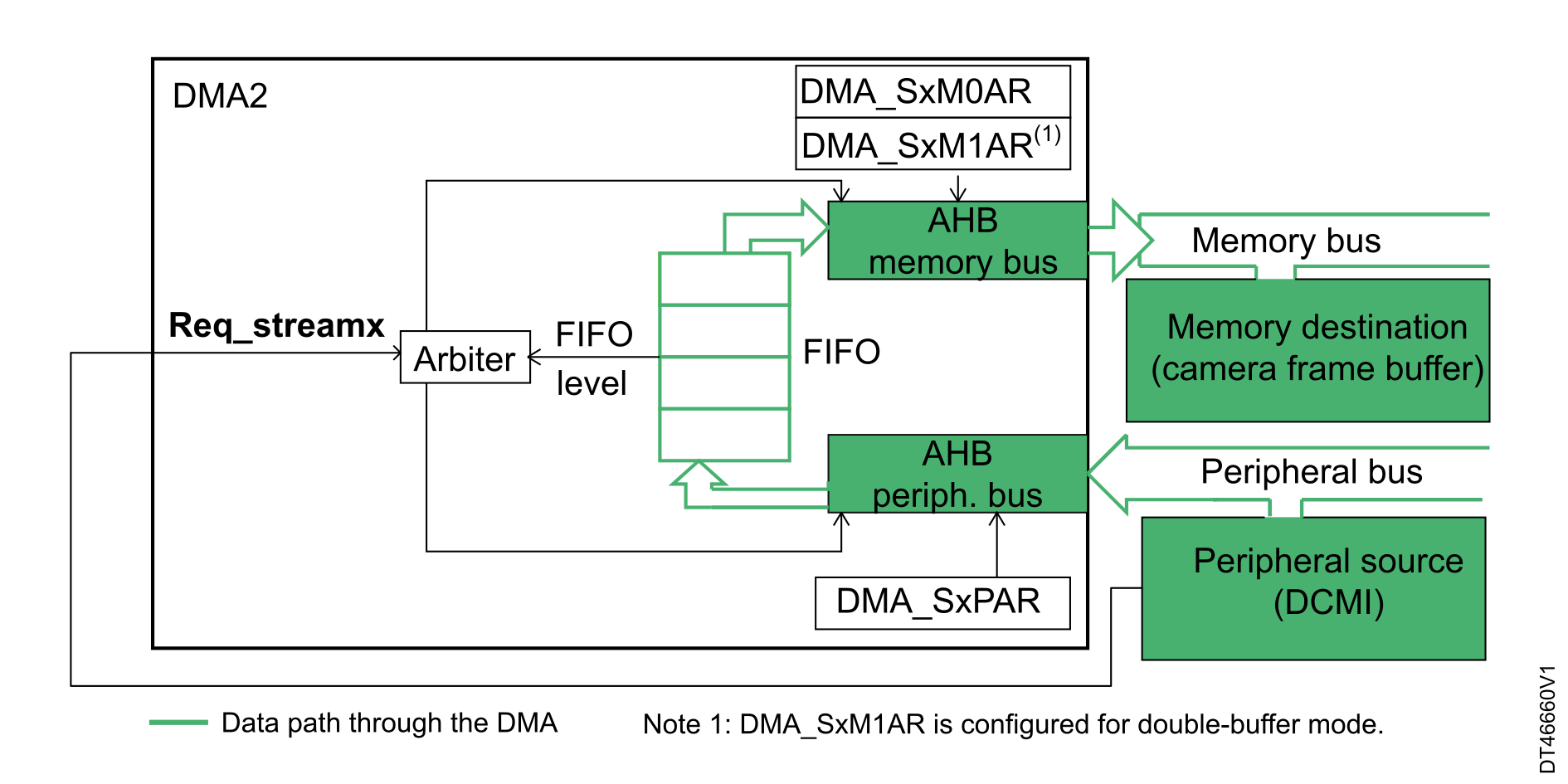
Figure 44 Data transfer through the DMA shows the DMA2 (or the DMA1 for STM32H7 and STM32L4+ devices, the GPDMA1 for the STM32U5, and STM32N647/657 devices, the GPDMA1 or the GPDMA2 for the STM32H5 devices) operation in peripheral-to-memory mode, except for the STM32L496xx and STM32L4A6xx devices. The DMA2 in these devices has only one port.
Figure 44. Data transfer through the DMA

DMA configuration versus image size and capture mode

The DMA must be configured according to the image size (color depth and resolution), and to the capture mode:

DCMI channel and stream configuration

The user must also configure the corresponding DMA2 (or the DMA1 for the STM32H7 and STM32L4+ devices, the GPDMA1 for the STM32U5 and STM32N647/657 devices, the GPDMA1 and GPDMA2 for the STM32H5 devices) stream and channel to ensure the DMA acknowledgment each time the DCMI data register is fulfilled.

The tables below summarize the DMA stream and channels that enable the DMA request from the DCMI.
Table 8. DMA stream selection across STM32 devices
STM32DMA streamChannel
STM32F2Stream 1 and stream 7Channel 1
STM32F4
STM32F7
STM32H7Stream 0 to stream 7Multiplexer 1 request 75
STM32L4Stream 0Channel 6
Stream 4Channel 5
Table 9. DMA stream selection across STM32 devices
STM32DMA channelRequest
STM32L4+STM32L4Rxxx and STM32L4SxxxChannel 1 to channel 7DMA request multiplexer 90
STM32L4P5xx and STM32L4Q5xxDMA request multiplexer 91
STM32U5Channel 0 to channel 15GPDMA1 request 86
STM32H5Channel 0 to channel 7GPDMA1/2 request 108
STM32N647/657Channel 0 to channel 15GPDMA1 request 140
Note:

See the reference manual for a step-by-step description of the stream and channel configuration procedure.

DMA_SxNDTR/DMA_CNDTRx/GPDMA_CxBR1 register

The total number of words to transfer from the DCMI to the memory is programmed in this register (see DMA configuration for DCMI-to-memory transfers).

When the DMA starts the transfer from the DCMI to the memory, the number of items decreases from the initial programmed value until the end of the transfer (reaching zero or disabling the stream by software before the number of data remaining reaches zero).

The table below gives the number of bytes corresponding to the programmed value and the peripheral data width (PSIZE bitfield).
Table 10. Maximum number of bytes transferred during one DMA transfer
Programmed value in the registerPeripheral sizeNumber of bytes
65535Words262140
0 < N < 355354 * N
Note:

To avoid data corruption, this programmed value must be a multiple of MSIZE or PSIZE.

FIFO and burst transfer configuration

The DMA performs the transfer with or without enabling the 4-word FIFO. When the FIFO is enabled, the source data width (programmed in PSIZE) can differ from the destination data width (programmed in MSIZE). In this case, the user must pay attention to adapt the address to write:
  • In DMA_SxPAR and DMA_SxM0AR (and DMA_SxM1AR in case of double-buffer mode configuration) to the data width programmed in PSIZE and MSIZE of DMA_SxCR for all STM32 except the STM32L4/L4+, STM32U5, STM32H5, and STM32N647/657 devices
  • In DMA_CPARx and DMA_CMARx to the data width programmed in PSIZE and MSIZE of DMA_CCRx for the STM32L4 and STM32L4+ devices
  • In GPDMA_CxSAR and GPDMA_CxDAR to the data width programmed with a burst length by SBL_1[5:0] (respectively DBL_1[5:0]), and with a data width defined by SDW_LOG2[1:0] (respectively DDW_LOG2[1:0]) in GPDMA_CxTR1 for the STM32U5, STM32H5, and STM32N647/657 devices

For a better performance, it is recommended to use the FIFO. When the FIFO mode is enabled, the user can configure the MBURST bits to make the DMA perform burst transfer (up to four words) from its internal FIFO to the destination memory, which guarantees better performance.

Normal mode for low resolution in snapshot capture

Low-resolution images are the ones having size (in 32-bit word) less than 65535. In snapshot mode, the normal mode can be used to ensure the transfer of low-resolution frames (see Table 10 Maximum number of bytes transferred during one DMA transfer).

The maximum number of pixels depends on the bit depth of the image (number of bytes per pixel). The DCMI supports two possible bit depths:
  • 1 byte per pixel in monochrome or Y only format
  • 2 bytes per pixel in case of RGB565 or YCbCr format
The table below summarizes the maximum image resolution that can be transferred using the normal mode.
Table 11. Maximum image resolution in normal mode
ItemMax number of bytesBit depth (byte/pixel)Max number of pixelsMax resolution
Word2621401262140720x364
2131070480x272

Circular mode for low resolution in continuous capture

The circular mode allows the process of successive frames (continuous data flows), providing that one frame size is less than 65535. The initial size value is programmed:
  • In DMA_SxNDTR for the STM32F2, STM32F4, STM32F7, and STM32H7 devices
  • In DMA_CNDTRx for the STM32L4x6 and STM32L4+ devices
  • In GPDMA_CxBr1 for the STM32U5, STM32H5, and STM32N647/657 devices

Each time the number of data decrementing reaches the zero, the number of data words is automatically reloaded to the initial value. Each time the DMA pointer reaches the end of the frame buffer, it is reinitialized, and the DMA ensures the transfer of the next frame.

The resolutions listed in Table 11 Maximum image resolution in normal mode are also valid for the low resolution in continuous mode.
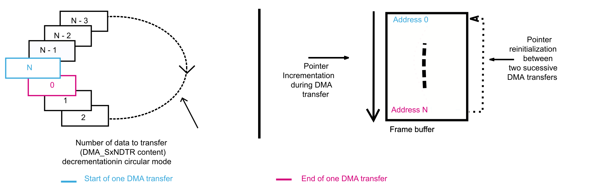
Figure 45 Frame buffer and DMA_SxNDTR register in circular mode shows the DMA_SxNDTR value and the frame buffer pointer modifications during a DMA transfer and between two successive DMA transfers.
Figure 45. Frame buffer and DMA_SxNDTR register in circular mode

Double-buffer mode for medium resolutions (snapshot or continuous capture)

Note:

This mode is not available for STM32L4A6xx and STM32L496xx devices.

Medium resolution images are the ones with a size (in 32-bit words) between 65536 and 131070. When the double-buffer mode is enabled, the circular mode is automatically enabled.

If the image size exceeds (in words) the maximum sizes mentioned in Table 11 Maximum image resolution in normal mode in snapshot or continuous capture, the double-buffer mode must be used in snapshot or continuous mode. In this case, the number of pixels per frame allowed is doubled since received data are stored in two buffers: each buffer maximum size (in 32-bit words) is 65535 (the maximum frame size is 131070 words or 524280 bytes). The images sizes and resolutions allowed to be received by the DCMI and transferred by the DMA are then doubled.
Table 12. Maximum image resolution in double-buffer mode
ItemMax number of bytesBit depth (byte/pixel)programmed value in the registerNumber of pixelsMax resolution
Word524280165535524280960x544
0 < N < 655358 * N
265535262140720x364
0 < N < 655354 * N
In this mode, the double-buffer stream has two pointers (two buffers for storing data), switched at each end of the transaction:
  • In snapshot mode, the DMA controller writes the data to the first frame buffer. After this first frame buffer is filled (at this level, the register is reinitialized to the programmed value, and the DMA pointer switches to the second frame buffer), the data is transferred to the second buffer. The total frame size (in words) is divided by two and programmed into the register. The image is stored to two buffers with the same size.
  • In continuous mode, each time one frame (image) is received and stored to the two buffers. As the circular mode is enabled, the register is reinitialized to the programmed value (total frame size divided by two), and the DMA pointer switches to the first frame buffer to receive the next frame.
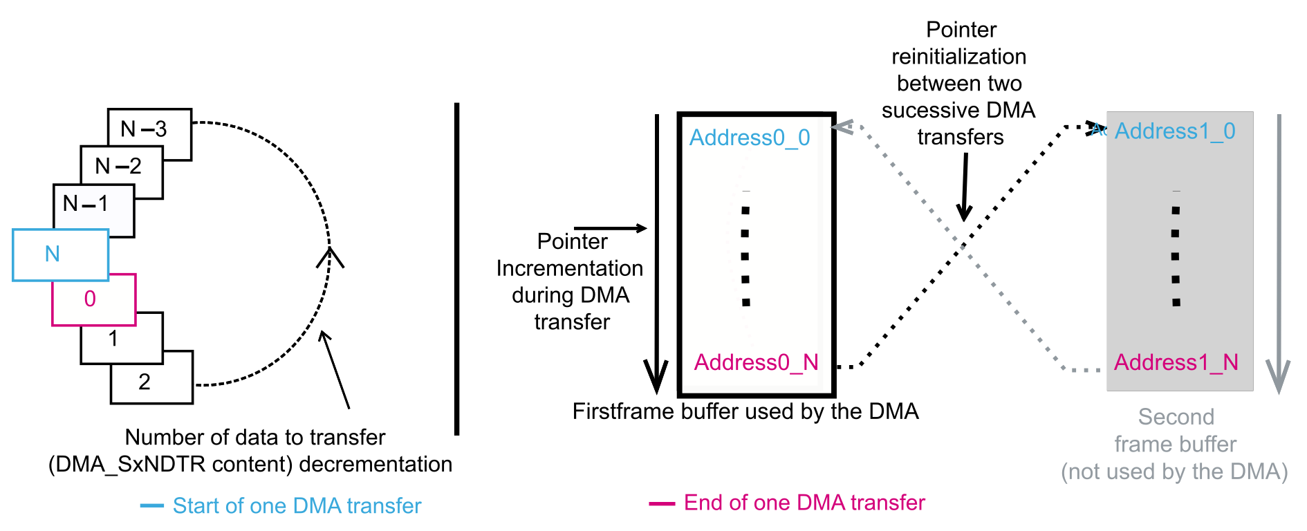
Figure 46 Frame buffer and DMA_SxNDTR register in double-buffer mode shows the two pointers and the DMA_SxNDTR value modifications during the DMA transfers.
Figure 46. Frame buffer and DMA_SxNDTR register in double-buffer mode

DMA configuration for higher resolutions

When the number of words in one frame (image) in snapshot or continuous mode exceeds 131070, and when the image resolution exceeds the indicated ones in Table 12 Maximum image resolution in double-buffer mode, the DMA double-buffer mode cannot ensure the transfer of the received data.

Note:

This section highlights only the DMA operation in case of high resolution. An example is developed and described using this DMA configuration in Resolution capture (YCbCr data format).

The STM32F2, STM32F4, STM32F7, STM32H7, and STM32L4+ devices embed a very important feature in double-buffer mode: the possibility to update the programmed address for the AHB memory port on-the-fly (in DMA_SxM0AR or DMA_SxM1AR) when the stream is enabled. The following conditions must be respected:
  • When CT is cleared to zero in DMA_SxCR (current target memory is memory 0), the DMA_SxM1AR register can be written. Attempting to write to this register while CT = 1 generates an error flag (TEIF), and the stream is automatically disabled.
  • When CT is set to one in DMA_SxCR (current target memory is memory 1), the DMA_SxM0AR register can be written. Attempting to write to this register while CT = 0 generates an error flag (TEIF), and the stream is automatically disabled.

To avoid any error condition, it is advised to change the programmed address as soon as the TCIF flag is asserted. At this point, the targeted memory must have changed from memory 0 to memory 1 (or from 1 to 0), depending on the CT bit value in DMA_SxCR.

Note:

For all the other modes than the double-buffer one, the memory address registers are write-protected as soon as the stream is enabled.

The DMA allows then the management of more than two buffers:
  • In the first cycle, while the DMA uses the buffer 0 addressed by pointer 0 (memory 0 address in DMA_SxM0AR), the buffer 1 is addressed by pointer 1 (memory 1 address in DMA_SxM1AR).
  • In the second cycle, while DMA uses the buffer 1 addressed by pointer 1, the buffer 0 address can be changed, and the frame buffer 2 can be addressed by pointer 0.
  • In the second cycle, while the DMA is using the buffer 2 addressed by pointer 0, the frame buffer 1 address can be changed, and the buffer 3 can be addressed by pointer 1.

DMA_SxM0AR and DMA_SxM1AR can then be used to address many buffers, ensuring the transfer of high resolution images.

Note:

To simplify the use of this specific feature, it is recommended to divide the image into equal buffers. When capturing high resolution images, the user must secure that the memory destination has a sufficient size.

Example: In case of a resolution that is 1280x1024, the image size is 655360 words (32 bits). This size must be divided into equal buffers, with a maximum size of 65535 for each of them. To be correctly received, the image must then be divided into 16 frame buffers, with each frame buffer size equal to 40960 (lower than 65535).
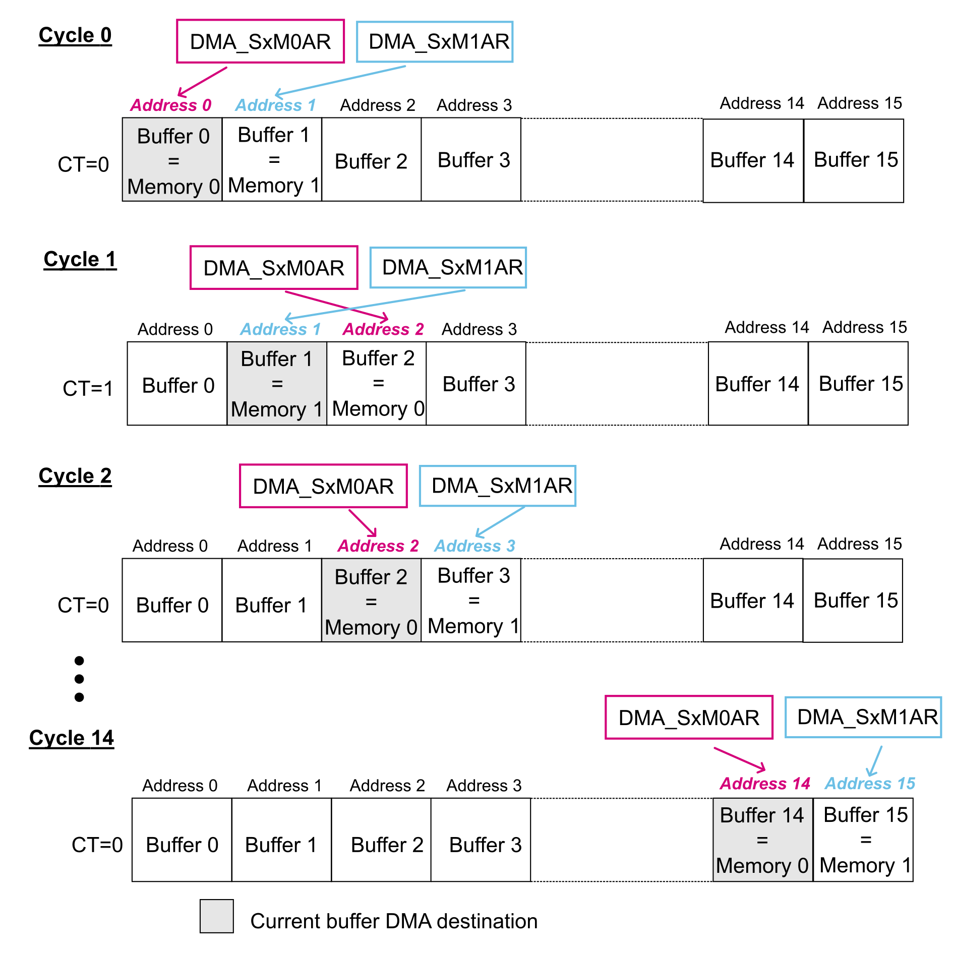
Figure 47 DMA operation in high resolution case illustrates the DMA_SxM0AR and DMA_SxM1AR update during the DMA transfer:
Figure 47. DMA operation in high resolution case