Readout protection (RDP)
The readout protection is a global flash memory protection allowing the embedded firmware code to be protected against copy, reverse engineering, dumping, using debug tools, or code injection in SRAM. The user must set this protection after the binary code is loaded to the embedded flash memory.
- The main flash memory
- The option bytes (level 2 only)
- Backup registers for real-time clock (RTC)
- Backup SRAM
- Nonvolatile memories
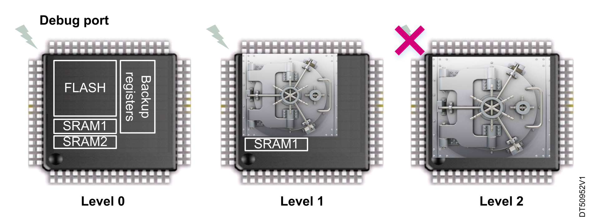
- Level 0(default RDP level)
The flash memory is fully open, and all memory operations are possible in all boot configurations (debug features, boot from RAM, boot from system memory bootloader, boot from flash memory). There is no protection in this configuration mode that is appropriate only for development and debug.
- Level 1
Flash memory accesses (read, erase, program), or SRAM2 accesses via debug features (such as serial-wire or JTAG) are forbidden, even while booting from SRAM or system memory bootloader. In these cases, any read request to the protected region generates a bus error.
However, when booting from flash memory, accesses to both flash memory and to SRAM2 (from user code) are allowed.
- Level 2
All protections provided in Level 1 are active, and the MCU is fully protected. The RDP option byte and most of the other option bytes are frozen, and can no longer be modified. The JTAG, SWV (single-wire viewer), ETM, and boundary scan are all disabled. The exception is STM32C5, which allows setting RDP2 with or without keeping boundary scan available for use.
- Level 0.5 (for nonsecure debug only)
All read and write operations (if no write protection is set) from/to the nonsecure flash memory are possible. The debug access to the secure area is prohibited. Debug access to nonsecure areas remains possible.
RDP level regression
- Regression from RDP level 1 to RDP level 0 leads to a flash memory mass erase, and the erase of SRAM2 and backup registers.
- Regression from RDP level 1 to RDP level 0.5 leads to a partial flash memory erase: only the nonsecure part is erased.
- Regression from RDP level 0.5 to RDP level 0 leads to a flash memory mass erase, and the erase of SRAM2 and backup registers.
In RDP level 2, except for preconfigured OEM keys in the STM32Ux and STM32C5 series, no regression is possible.
Internal flash memory content updating on an RDP protected STM32 MCU
In RDP level 1 or 2, the flash memory content can no longer be modified with an external access (bootloader or booting from SRAM). However, modifications by an internal application are always possible. Practical implementations of such firmware updates are SFU (secure firmware update) and IAP (in‑application‑programming). See examples in related documents AN4657 AN5156_General-Info.html#concept_vts_yqx_fcb__ph_18, AN5056 AN5156_General-Info.html#concept_vts_yqx_fcb__ph_19, AN5544 AN5156_General-Info.html#concept_vts_yqx_fcb__ph_20, and AN5447 AN5156_General-Info.html#concept_vts_yqx_fcb__ph_7 to learn more.
Regression locked by OEM keys
The STM32C5, STM32U0, and STM32U5 series introduce the possibility to define secret keys (passwords) to allow controlled regression (for example for fault analysis purposes). The keys are programmed in a similar way as a regular option byte, and to allow regression, they need to be presented to the debug interface in a dedicated connection mode, which prevents concurrent connection for normal debug session.
There are separate keys for regression from RDP2 and from RDP1.
Regression is supported in the STM32CubeProgrammer utility both in GUI and CLI.
| Area | RDP level | Boot from user flash memory | Debug or boot from SRAM or from bootloader | ||||
|---|---|---|---|---|---|---|---|
| Read | Write | Erase | Read | Write | Erase | ||
| Flash main memory | 0 | Yes | Yes | Yes | Yes | Yes | Yes |
| 1 | Yes | Yes | Yes | No | No | No | |
| 2 | Yes | Yes | Yes | N/A | N/A | N/A | |
| System memory | 0 | Yes | No | No | Yes | No | No |
| 1 | Yes | No | No | No | No | No | |
| 2 | Yes | No | No | N/A | N/A | N/A | |
| Option bytes | 0 | Yes | Yes | Yes | Yes | Yes | Yes |
| 1 | Yes | Yes | Yes | Yes | Yes | Yes | |
| 2 | Yes | No | No | N/A | N/A | N/A | |
| Other protected assets 1 | 0 | Yes | Yes | Yes | Yes | Yes | Yes |
| 1 | Yes | Yes | N/A | No | No | No | |
| 2 | Yes | Yes | N/A | N/A | N/A | N/A | |
When to use the RDP
On a consumer product, the RDP must always be set at least at level 1. This prevents basic attacks through the debug port or through the bootloader. However, in RDP level 1, there is a risk of service denial caused by a flash memory mass erase, following a return to RDP level 0.
The RDP level 2 is mandatory to implement an application with a higher security level (such as immutable code). The drawback is that the RDP level 2 can prevent a device examination, for instance after a customer return.
The RDP level 0.5 is used to debug a nonsecure application, while protecting contents within secure area boundaries from debug access. Refer to section 'Development recommendations using TrustZone®' of the application note Arm® TrustZone® features on STM32L5 and STM32U5 series (AN5347) for more information about this protection.
The RDP is available on all STM32 device, unless succeeded by the life cycle management product state (see Life cycle management–product state).