LTDC in a smart architecture
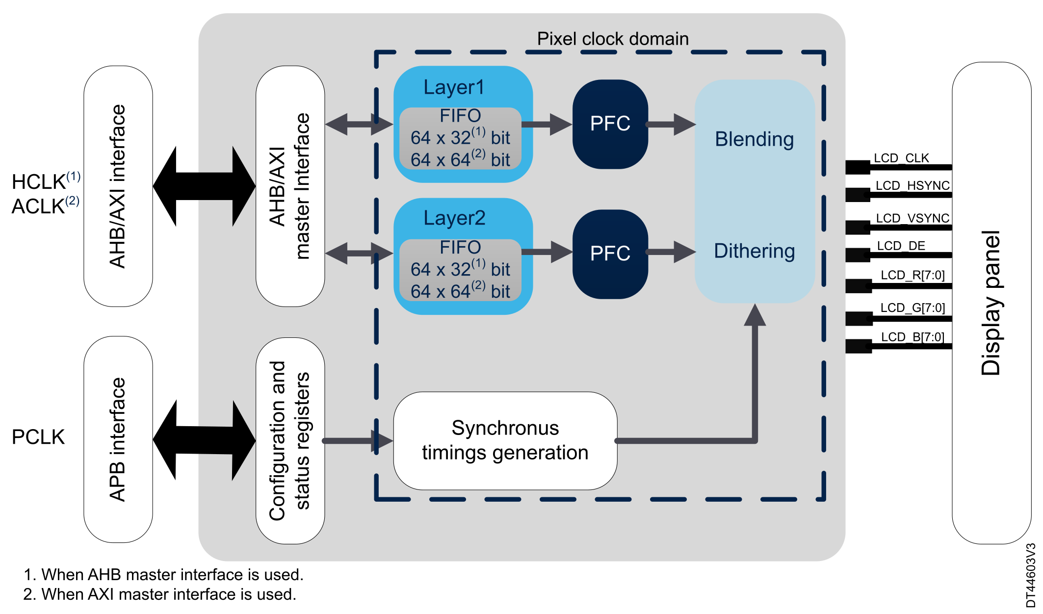
The LTDC is a master on the AHB/AXI architecture that performs read access on internal and external memories. The LTDC has two independent layers, each one with its own FIFO enabling more flexibility of the display.
The LTDC controller autonomously fetches graphical data at the speed of the AHB/AXI bus from the framebuffer. The graphical data is then stored in one of the internal layers FIFO then driven to the display.
The system architecture allows graphics to be built and plotted to the screen without any CPU intervention. The LTDC retrieves the data belonging to an image from the framebuffer, while the DMA2D prepares the next images.
The LTDC interface is integrated in a smart architecture allowing:
- LTDC autonomously fetches the graphical data from the framebuffer (can be internal memories such as internal flash, internal SRAM or external memories, such as FMC_SDRAM or Quad-SPI) and drives it to the display.
- DMA2D, as an AHB/AXI master, can be used to offload the CPU from graphics intensive tasks.
- LTDC is able to continue displaying graphics even in Sleep mode when the CPU does not run.
- The multilayer AHB/AXI bus architecture improves memories throughput and leads to higher performance.
System architecture on STM32F429/439 and STM32F469/479 microcontrollers
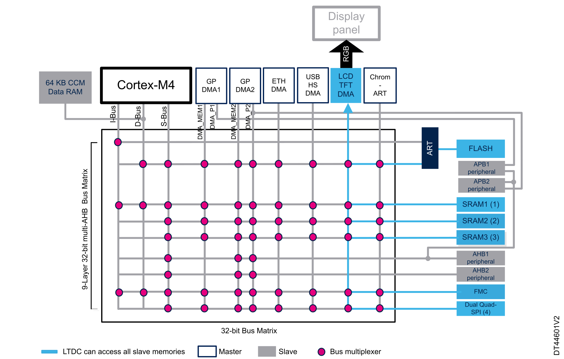
The system architecture of the STM32F429/439 line and the STM32F469/479 line consists mainly of 32-bit multilayer AHB bus matrix that interconnects ten masters and nine slaves (eight slaves for the STM32F429/F439). The LTDC is one of the ten AHB masters on the AHB bus matrix.
The LTDC can autonomously access all the memory slaves on the AHB bus matrix, such as FLASH, SRAM1, SRAM2, SRAM3 FMC or Quad-SPI enabling an efficient data transfer that is ideal for graphical applications.
Figure 9 LTDC AHB master in STM32F429/439 and STM32F469/479 smart architecture. (1) SRAM1 size = 112 Kbytes for STM32F429/439 and 160 Kbytes for STM32F469/479. (2) SRAM2 size = 16 Kbytes for STM32F429/439 and 32 Kbytes for STM32F469/479. (3) SRAM3 size = 64 Kbytes for STM32F429/439 and 128 Kbytes for STM32F469/479. (4) Dual Quad-SPI interface is only available for STM32F469/479. shows the LTDC interconnection in the STM32F429/439 and STM32F469/479 lines systems.
(1) SRAM1 size = 112 Kbytes for STM32F429/439 and 160 Kbytes for STM32F469/479.
(2) SRAM2 size = 16 Kbytes for STM32F429/439 and 32 Kbytes for STM32F469/479.
(3) SRAM3 size = 64 Kbytes for STM32F429/439 and 128 Kbytes for STM32F469/479.
(4) Dual Quad-SPI interface is only available for STM32F469/479.
System architecture on STM32F7x6, STM32F7x7, STM32F7x8, and STM32F7x9
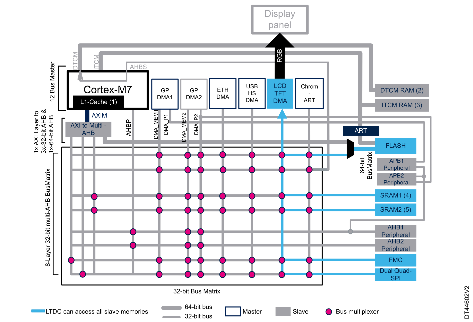
The system architecture of the STM32F7x6, STM32F7x7, STM32F7x8, and STM32F7x9 consists mainly of 32-bit multilayer AHB bus matrix that interconnects twelve masters and eight slaves. The LTDC is one of the twelve AHB masters on the AHB bus matrix.
The LTDC can autonomously access all the memory slaves on the AHB bus matrix, such as FLASH, SRAM1, SRAM2, FMC, or Quad-SPI enabling an efficient data transfer that is ideal for graphical applications. Figure 10 LTDC AHB master in STM32F7x6, STM32F7x7, STM32F7x8, and STM32F7x9 smart architecture. (1) I/D Cache size = 4 Kbytes for STM32F7x6. I/D Cache size = 16 Kbytes for STM32F7x7, STM32F7x8, and STM32F7x9. (2) DTCM RAM size = 64 Kbytes for STM32F7x6. DTCM RAM size = 128 Kbytes for STM32F7x7, STM32F7x8, and STM32F7x9. (3) ITCM RAM size = 16 Kbytes for STM32F7x6, STM32F7x7, STM32F7x8, and STM32F7x9. (4) SRAM1 size = 240 Kbytes for STM32F7x6. SRAM1 size = 368 Kbytes for STM32F7x7, STM32F7x8, and STM32F7x9. (5) SRAM2 size = 16 Kbytes for STM32F7x6, STM32F7x7, STM32F7x8, and STM32F7x9. shows the LTDC interconnection in the STM32F7x6, STM32F7x7, STM32F7x8, and STM32F7x9 systems.
(1) I/D Cache size = 4 Kbytes for STM32F7x6.
I/D Cache size = 16 Kbytes for STM32F7x7, STM32F7x8, and STM32F7x9.
(2) DTCM RAM size = 64 Kbytes for STM32F7x6.
DTCM RAM size = 128 Kbytes for STM32F7x7, STM32F7x8, and STM32F7x9.
(3) ITCM RAM size = 16 Kbytes for STM32F7x6, STM32F7x7, STM32F7x8, and STM32F7x9.
(4) SRAM1 size = 240 Kbytes for STM32F7x6.
SRAM1 size = 368 Kbytes for STM32F7x7, STM32F7x8, and STM32F7x9.
(5) SRAM2 size = 16 Kbytes for STM32F7x6, STM32F7x7, STM32F7x8, and STM32F7x9.
System architecture on STM32H7Rx/7Sx
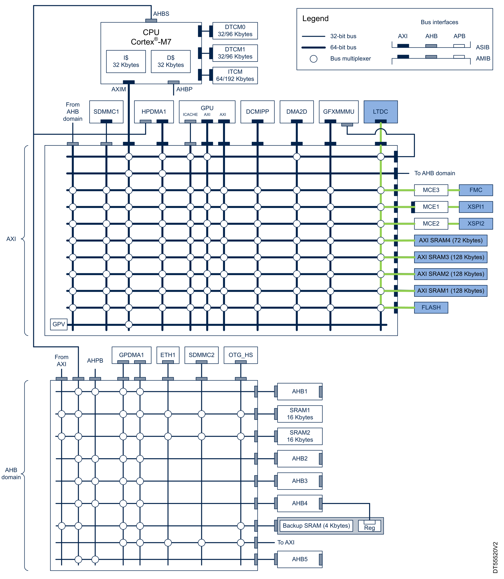
The system architecture of the STM32H7Rx/7Sx primarily consists of a 64-bit AXI, a 32-bit multilayer AHB bus matrix, and bus bridges that allow interconnection of bus masters with bus slaves. The AXI bus matrix connects 11 masters and 10 slaves. The LTDC is one of the 11 AXI masters on the AXI bus matrix. The LTDC can autonomously access all the memory slaves on the AXI bus matrix, such as FLASH, AXI SRAM1, AXI SRAM2, AXI SRAM3, AXI SRAM4, FMC, or XSPI, enabling efficient data transfer ideal for graphical applications.