This section illustrates the different steps required before and during a graphical application development using LTDC. The user must at first determine the graphical application requirements, then check if the desired display size fits the hardware configuration. During the graphical application compatibility check phase, the existing STM32 reference boards described in AN4861_Reference-boards-with-LCD-TFT-panel.html#id_61973__table_wcq_hcr_31c can be used to evaluate his hardware and software configuration.
Determining graphical application requirements
Determining the graphical application needs is a crucial step to start from. Some of the most important parameters to be defined before starting the creation of the graphical application are display resolution, color depth, as well as the nature of the data to display (static images, text, or animation).
Once the basic parameters mentioned above are defined, the user must determine the graphical hardware architecture of the application, as well as the required hardware resources. The best-fitting STM32 package (see Table 21 STM32 packages with LTDC peripheral versus RGB interface availability) must be selected, according to the following parameters:
If an external memory is needed for the framebuffer.
The external framebuffer memory bus width
The LTDC interface: RGB565, RGB666, or RGB888 depending on the display module
If an external memory is needed to store graphic primitives (serial NOR flash, parallel NOR flash).
Checking the display size and color depth compatibility with the hardware configuration
When starting a graphic application development using an STM32 microcontroller, the user has often a defined desired display size and color depth. A key question that the user must answer before continuing the development is if such display size and color depth match a specific hardware configuration.
The following steps are needed in order to answer this question:
Determine the required framebuffer size and its location.
Check the compatibility of the display versus the framebuffer memory bandwidth requirements.
Check the compatibility of the display panel interface with the LTDC.
Framebuffer memory size requirements and location
Determining the framebuffer memory size and its location is a key parameter for the display compatibility check.
The memory space required in the RAM to support the framebuffer must be contiguous and with a minimum size equal to:
Framebuffer size = number of pixels x bits per pixel
As shown in the formula above, the required framebuffer size depends on the display resolution and on its color depth.
It is not necessary that the framebuffer color depth (bpp) is the same than the display color depth. For instance, an RGB888 display can be driven using an RGB565 framebuffer.
Note:
The required framebuffer size is doubled for double-framebuffer configuration. It is common to use a double-buffer configuration where one graphic buffer is used to store the current image, while the second buffer is used to prepare the next image.
Depending on the required framebuffer size, the framebuffer can be located either in an internal SRAM or in an external SRAM/SDRAM.
If the internal RAM is not enough for the framebuffer, the user must use either an external parallel SDRAM/SRAM/PSRAM connected to FMC or external serial SRAM/PSRAM connected to XSPI.
Consequently, the required framebuffer size determines if the use of an external memory is needed or not. The required framebuffer size depends on the display size and color depth.
Locating the framebuffer in the Internal SRAM
Depending on the framebuffer size, the framebuffer can be placed either in the internal SRAM or the external RAM.
Using an internal SRAM as a framebuffer allows the maximum performances and avoids any bandwidth limitation issues for the LTDC.
Using the internal SRAM instead of an external RAM has many advantages:
higher throughput (0 wait state access)
reduced number of required pins and PCB design complexity
reduced BOM, hence cost, since no external memory is needed
The only limitation when using the internal SRAM is its limited size (hundreds of Kbytes). When the framebuffer size exceeds the available memory, an external RAM (driven by the FMC or XSPI interface) must be used. However, when dealing with external memories, the user must be careful to avoid bandwidth limitation. For more detailed information, refer to Graphic performance optimization.
Note:
The color look-up table CLUT can be used to decrease the required framebuffer size. (For more details, refer to the STM32 MCU reference manual).
1 The required framebuffer size is doubled for double-framebuffer configuration.
2 An example of a custom 480 x 272 display is the ROCKTECH embedded on the STM32F746 discovery kit (32F746GDISCOVERY).
Checking display compatibility considering the memory bandwidth requirements
This section explains how to check a display compatibility considering the framebuffer memory bandwidth. Some important bandwidth aspects are described and this section explains how to determine the required bandwidth for the pixel clock and the LTDC. Finally, a simple method to conclude whether a desired display size is compatible with a specific hardware configuration; is detailed.
Framebuffer memory bandwidth aspects
Once the framebuffer location is fixed (either in internal or external memory), the user must check if its bandwidth can sustain the hardware configuration.
To check if the memory bandwidth can sustain the LTDC required bandwidth, the user must consider any other concurrent accesses to the memory.
In general, a small size framebuffer located in the internal RAM does not require a high bandwidth. This is because a small size framebuffer means low pixel clock, hence low LTDC required bandwidth.
A more complex use case to analyze is when the framebuffer is located in an external memory.
Framebuffer memory bus concurrency
LTDC, DMA2D, and CPU masters.
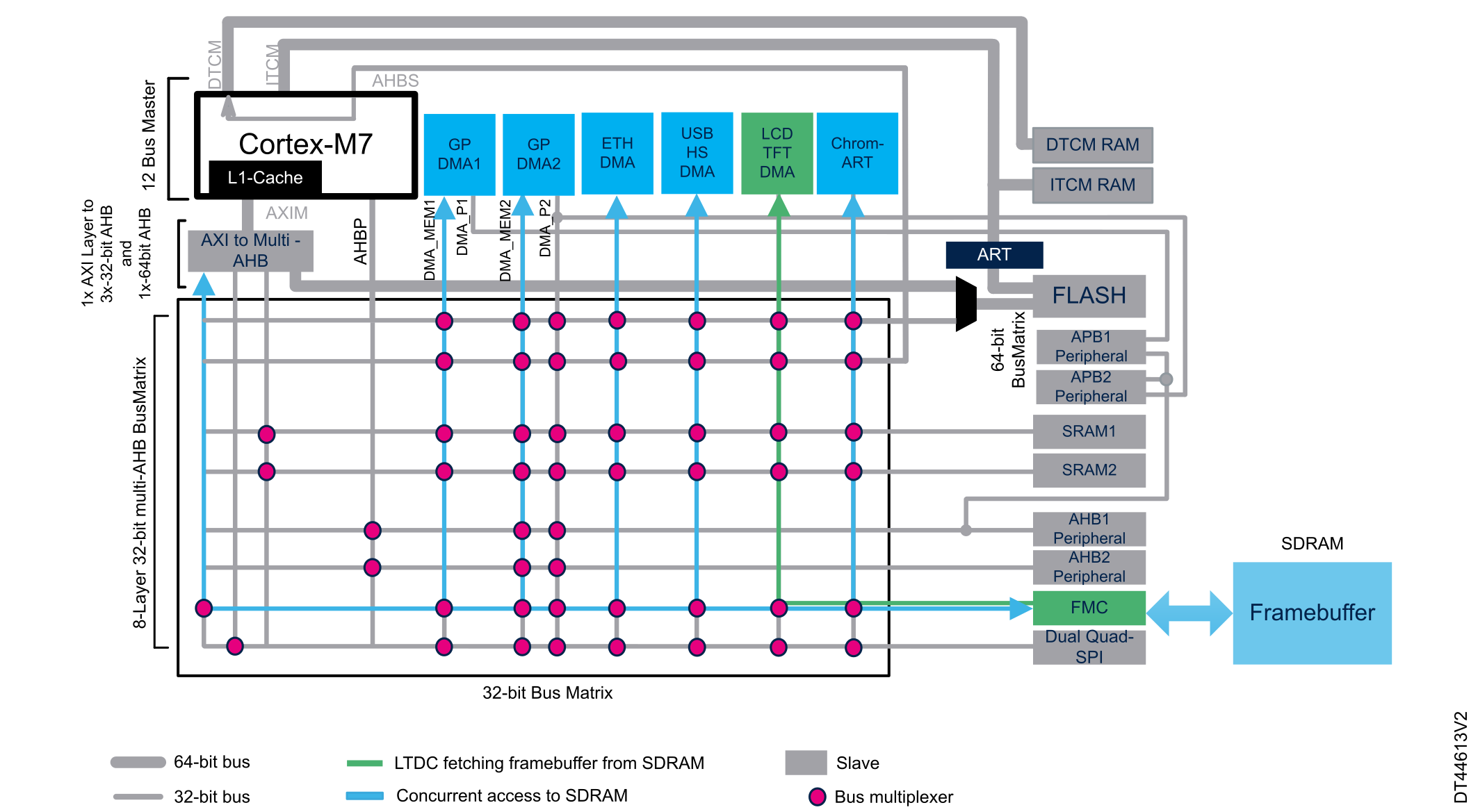
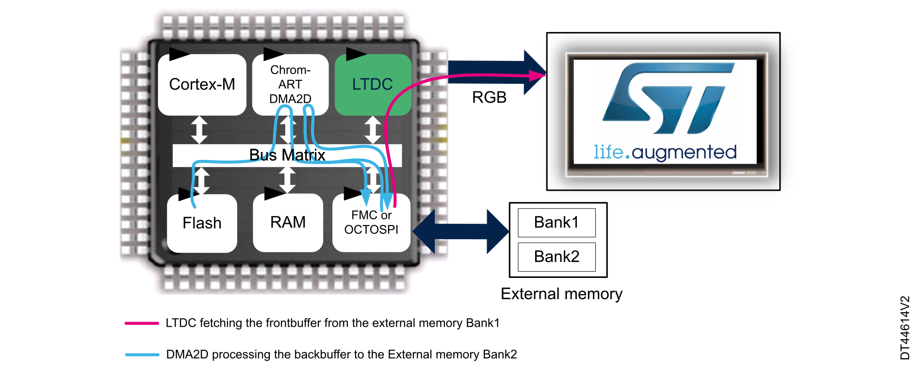
In a typical graphic application where an external RAM is used as framebuffer, two or three main AHB masters concurrently use the same memory.
The DMA2D (or the CPU) updates the next image to be displayed while the LTDC fetches and displays the actual image. The memory bus load depends mainly on the LTDC required bandwidth.
Other AHB/AXI masters.
It is common that an external RAM is shared by other masters and not only by those used for graphics. This concurrency leads to heavy bus load and may impact the graphic performances.
When locating the framebuffer in an external SDRAM/SRAM, the user must consider that the external memory running frequency is around half or third of the system frequency. That is the reason why the memory bandwidth must be considered as the bottleneck of the whole graphic system.
One of the needed parameters for checking the display compatibility is the memory bus width. For SDRAM, an 8-bit, 16-bit, or 32-bit configuration can be used.
As previously stated, the most complex to analyze is the use case when the framebuffer is placed in an external memory:
The masters concurrent access on the same external memory leads to more latency and impacts its throughput.
Determining pixel clock and LTDC required bandwidth
Pixel clock computation
The pixel clock is a key parameter for checking display size compatibility with a specific hardware configuration.
To get the typical pixel clock of the display, refer to the display datasheet. The computed pixel clock need to respect the display specifications.
The pixel clock for a specific refresh rate is calculated with the following formula: LCD_CLK (MHz) = total screen size x refresh rate Where total screen size = total width x total height.
LTDC required bandwidth
The LTDC required bandwidth depends mainly on three factors:
Number of used LTDC layers.
LTDC layer color depth.
Pixel clock (depends on the resolution of the display panel and on the refresh rate).
The maximum required bandwidth can be calculated as described below:
If only one LTDC layer is used: LTDC required bandwidth = LCD_CLK x BppL1
If two LTDC layers are used: LTDC required bandwidth = LCD_CLK x (BppL1 + BppL2)
Where BppL1 and BppL2 are respectively the color depth for LTDC Layer1 and Layer2. The LTDC required bandwidth must not exceed the memory available bandwidth, otherwise, display problems may occur and the FIFO underrun flag may be set (if the FIFO underrun interrupt was enabled). Note: If the memory used to store the framebuffer is also used for other application purposes, it may impact the graphical performances of the system.
Check if the used display resolution fits the hardware configuration
The general method for checking whether a display size with a particular color depth is compatible with memory bandwidth includes the following steps:
Compute the pixel clock according to the display size or extract it from the display datasheet.
Used system clock speed HCLK/ACLK and framebuffer memory speed.
External framebuffer memory bus width.
Number of AHB/AXI masters accessing concurrently to external framebuffer memory.
The user must perform some tests to confirm the hardware compatibility with the desired display size and color depth. To do it, the user must monitor the LTDC FIFO underrun interrupt flag in the LTDC_ISR register.
If the FIFO underrun interrupt flag is always reset, then the user confirms that the desired display size is compatible with the hardware configuration.
If the FIFO underrun flag is set, the user must check the following points:
If the FIFO underrun is still set because there are more than two master concurrent accesses to the external memory, the user must relax the memory bandwidth using the below recommendations:
Use only one LTDC layer.
Use the largest possible memory bus width (32-bit instead of 16- or 8-bit SDRAM/SRAM).
Update the framebuffer content during the blanking period when the LTDC is not fetching.
Use the highest possible system clock HCLK/ACLK and the highest memory speed.
Figure 23 Typical graphic hardware configuration with external SDRAM shows a typical graphic hardware configuration where an external SDRAM is connected to the FMC that is used for framebuffer. The SDRAM memory bandwidth depends on the bus width and in the operating clock.
The SDRAM bus width can be 32-bit, 16-bit, or 8-bit, while the operating clock depends on the system clock HCLK and the configured prescaler (HCLK/2 or HCLK/3).
Figure 23. Typical graphic hardware configuration with external SDRAM
For STM32N6xx devices, the AXI QOS is set to maximum for LTDC. As a consequence, the maximal supported pixel clock is the same for both LTDC and LTDC+DMA2D tests. The values are limited by the LTDC Kernel clock at 88 MHz.
Example of supported display resolutions for STM32F4x9 and STM32F7x6/7/8/9
1 System clock HCLK = 180 MHz, SDRAM runs at 90 MHz.
2 LTDC fetches the front buffer from the external memory. Either only one LTDC layer or two layers are used. The LTDC layer color depth is 8, 16, 24, or 32 bpp.
3 LTDC fetches the front buffer from the external memory while the DMA2D transfers data from backbuffer to frontbuffer.
4 System clock HCLK = 200 MHz, SDRAM runs at 100 MHz.
5 LTDC fetches the front buffer from the external memory. Either only one LTDC layer or two layers are used. The LTDC layer color depth is 8, 16, 24, or 32 bpp.
6 LTDC fetches the front buffer from the external memory while the DMA2D transfers data from backbuffer to frontbuffer.
11 LTDC fetches the front buffer from the external memory. The LTDC layer color depth is 8, 16, 24, or 32 bpp.
12 LTDC fetches the front buffer from the external memory while the DMA2D transfers data from backbuffer to frontbuffer.
13 ACLK = 300 MHz, PSRAM runs at 200MHz, SDRAM runs at 100 MHz
14 LTDC fetches the front buffer from the external memory. The LTDC layer color depth is 8, 16, 24, or 32 bpp.
15 When the LTDC and DMA2D have the same read QoS priority (default configuration for H7RS), the LTDC fetches the front buffer from the external memory while the DMA2D prepares the back buffer.
34 Up to 8 bpp for the STM32F4x9 microcontrollers.
Check the compatibility of the display panel interface with the LTDC
The user must choose the LCD panel depending on the application needs. The two main factors to consider when choosing the LCD panel are the resolution and the color depth. These two factors have a direct impact on the following parameters:
required GPIO number
framebuffer size and location
pixel clock of the display
When selecting a display panel, the user must:
Ensure that the display interface is compatible with the LTDC (parallel RGB with control signals).
Check if the control signals can be controlled by the LTDC (additional GPIOs are sometimes needed).
Ensure that the display signal levels are matching the LTDC interface signal levels (VDD from 1.8 V to 3.6 V).
Ensure that the display pixel clock is supported by the LTDC maximum pixel clock defined in the relevant STM32 product datasheet.