Example: creating a basic graphical application
This section provides an example based on the STM32F746G-DISCO board, describing the steps required to create a basic graphic application.
This section provides an example based on the STM32F746G-DISCO board, describing the steps required to create a basic graphic application.
The hardware resources embedded on the STM32F746G-DISCO board are used in this example. Figure 34 Graphic hardware configuration in the STM32F746G-DISCO. The pink arrow shows the pixel data path to the display. describes the graphic hardware resources to be used:
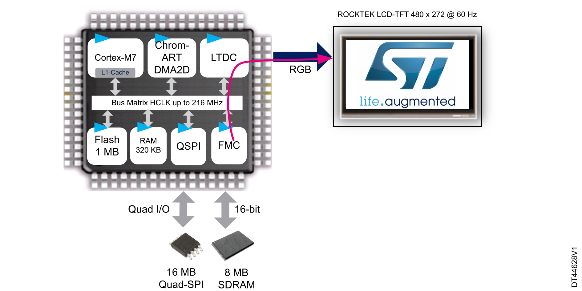
The STM32F746G-DISCO board embeds a parallel true color RGB888 LCD-TFT panel with a 480 x 272 resolution.
For more details on the STM32F746G-DISCO board, refer to the document AN4861_General-information.html#id_62127__entry_h3v_zmy_31c.
Figure 35 LCD-TFT connection in the STM32F746G-DISCO board shows the ROCKTECH RK043FN48H true color panel (RGB888) connected to the STM32F746 MCU.
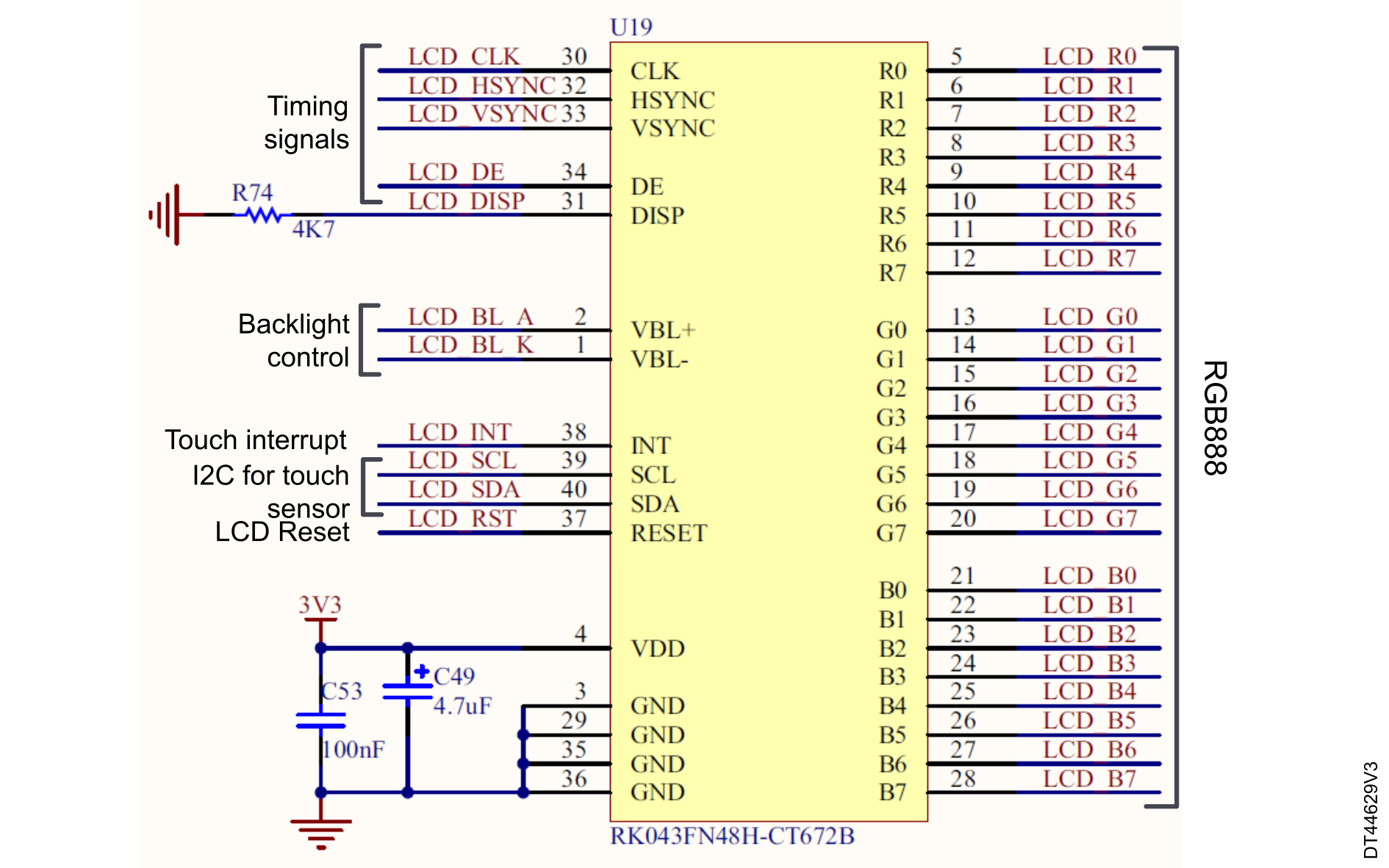
As shown in the last figure, the display module is connected to the MCU through two different pin categories:
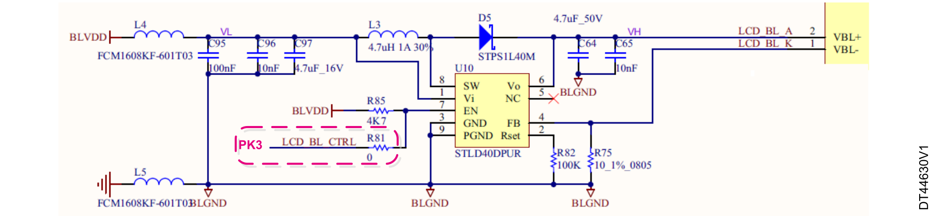
Backlight controller: the STLD40DPUR circuit described in Figure 36 Backlight controller module is a boost converter that operates from 3.0 V to 5.5 V. It can provide an output voltage as high as 37 V and can drive up to ten white LEDs in series. Refer to the STLD40D datasheet for more information on the backlight controller.
The high level on the LCD_BL_CTRL (PK3) signal lights the backlight on, while the low level switches it off.
It is possible to change the display brightness (dim the backlight intensity) by applying a low-frequency(1 to 10 kHz) PWM signal to the EN pin 7 of the STLD40D circuit. This action needs a rework since there is no timer PWM output alternate function available on the PK3 pin. The user must remove the R81 resistance and connect another GPIO pin with the PWM output alternate function.
This section uses a desired display size of 480 x 272 at 60Hz and with a 24 bpp color depth as reference to select the right hardware configuration.
The desired display is the ROCKTECH RK043FN48H-CT672B display:
Depending on its size and on the internal available SRAM size, the framebuffer can be located either in the internal SRAM or in the external SDRAM. The total embedded SRAM size for the STM32F746NGH6 MCU is 320 Kbytes where SRAM1 (240 Kbytes) can be used (see Figure 10 LTDC AHB master in STM32F7x6, STM32F7x7, STM32F7x8, and STM32F7x9 smart architecture. (1) I/D Cache size = 4 Kbytes for STM32F7x6. I/D Cache size = 16 Kbytes for STM32F7x7, STM32F7x8, and STM32F7x9. (2) DTCM RAM size = 64 Kbytes for STM32F7x6. DTCM RAM size = 128 Kbytes for STM32F7x7, STM32F7x8, and STM32F7x9. (3) ITCM RAM size = 16 Kbytes for STM32F7x6, STM32F7x7, STM32F7x8, and STM32F7x9. (4) SRAM1 size = 240 Kbytes for STM32F7x6. SRAM1 size = 368 Kbytes for STM32F7x7, STM32F7x8, and STM32F7x9. (5) SRAM2 size = 16 Kbytes for STM32F7x6, STM32F7x7, STM32F7x8, and STM32F7x9.).
The framebuffer size is calculated in the following way:
Based on these results, the required framebuffer size is about 128 Kbytes for 8 bpp. In that case, the framebuffer can be located in the internal SRAM1 (240 Kbytes). This is not valid for a double-framebuffer case as the size of 128 x 2 Kbytes exceeds the internal SRAM size.
For the 16 bpp color depth and in a double-framebuffer configuration, the required framebuffersize (2 x 255 Kbytes) exceeds the internal SRAM size, so using an external SRAM or SDRAM is a must for this configuration.
For the 24 bpp color depth and in a double-framebuffer configuration, the required framebuffersize exceeds the internal SRAM size (2 x 382.5 Kbytes), so using an external SRAM, or SDRAM is a must for this configuration.
The next step is to check if the SDRAM 16-bit bus width can sustain the desired resolution and color depth.
At this stage, the user decided to use an external SDRAM but still has to check if the SDRAM16-bit bus width (actual hardware implementation in the discovery board) matches the 480 x 272 @ 60 Hz display size and 24 bpp color depth.
In order to conclude if such hardware configuration can support the desired display size and color depth or not, the user must first compute the pixel clock.
The computed LCD_CLK is about 9.5 MHz (for computing pixel clock refer to AN4861_LTDC-peripheral-configuration-1.html#id_61969__b_o3v_jcl_yhc.
Then the user must check, based on the following parameters, if the computed pixel clock is not higher than the maximum LCD_CLK indicated in Table 11 STM32F7x6/7/8/9 maximal supported pixel clock:
Referring to the pixel clock Table 11 STM32F7x6/7/8/9 maximal supported pixel clock in the “LTDC + DMA2D” column and one layer row, the pixel clock can reach 34 MHz for a 16-bit SDRAM.
So, the 16-bit SDRAM bus width is quite enough to sustain a 480 x 272 @ 60 Hz resolution (LCD_CLK = 9.5 MHz) with 24 bpp color depth.
As shown on Figure 35 LCD-TFT connection in the STM32F746G-DISCO board, the ROCKTECH RK043FN48H display is connected to the STM32F746xx using a parallel RGB888 of 24 bits.
Once that the STM32CubeMX project is created, in the Pinout tab, choose one from the listed hardware configurations. Figure 37 STM32CubeMX: LTDC GPIOs configuration shows how to select the RGB888 hardware configuration with the STM32CubeMX.
The user can also configure all the GPIOs by setting the right alternate function for each GPIO one by one.

If after selecting one hardware configuration (RGB888 as shown in the above figure), the used GPIOs do not match with the display panel connection board, the user can change the desired GPIO and configure the alternate function directly on the pin. Figure 38 STM32CubeMX: PJ7 pin configuration to LTDC_G0 alternate function shows how to configure manually a PJ7 pin to LTDC_G0 alternate function.
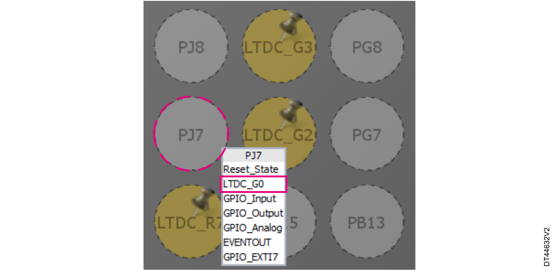
The used pins are highlighted in green once all LTDC interface GPIOs are correctly configured. The user must now set their speed to very high.
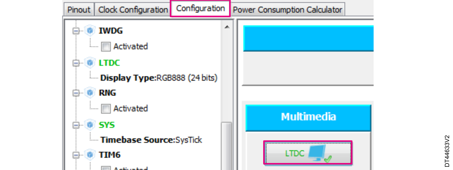
To set the GPIOs speed using STM32CubeMX, select the Configuration tab then click on the LTDC button as shown in Figure 39 STM32CubeMX: LTDC configuration.
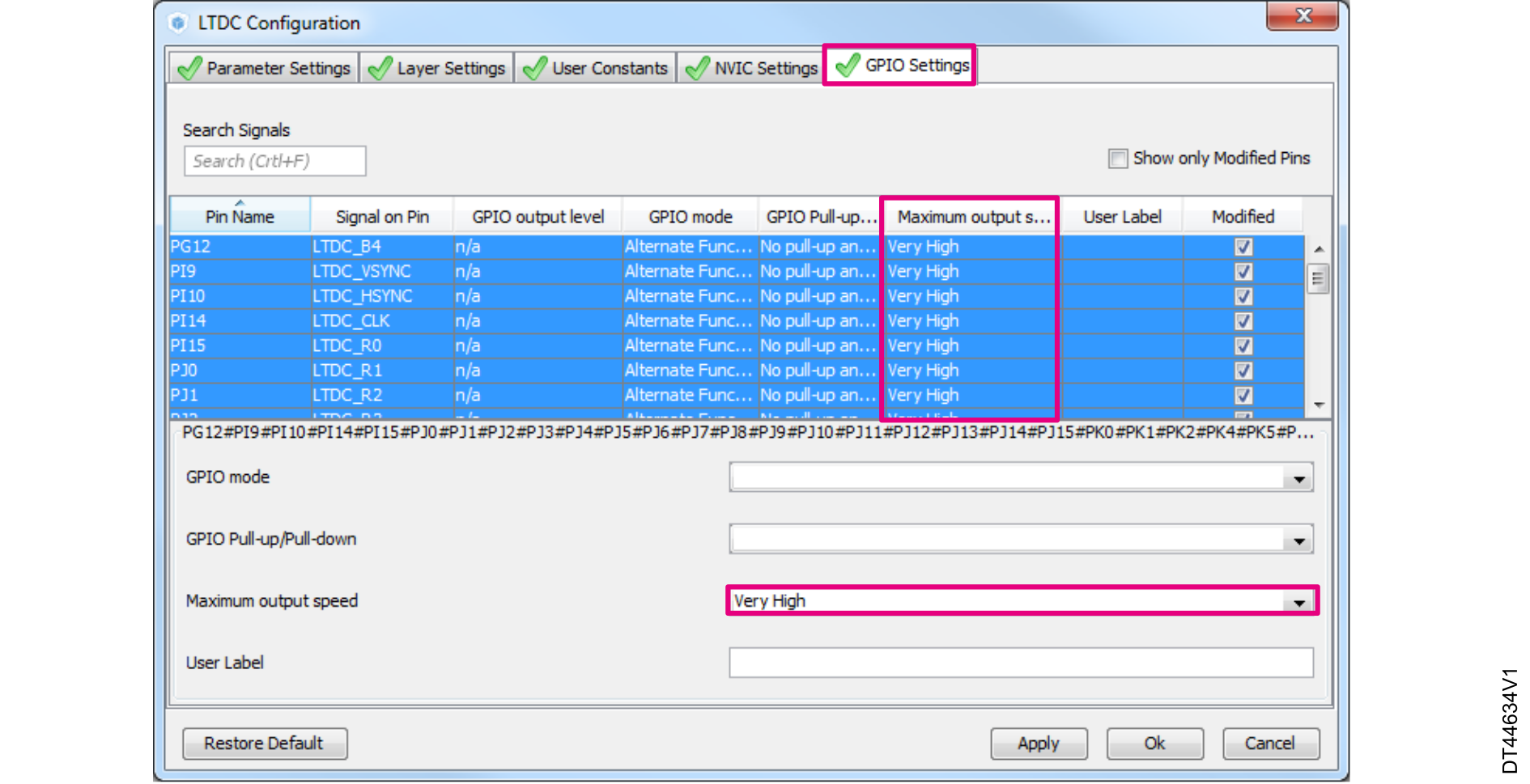
In the LTDC Configuration window described in Figure 40 STM32CubeMX: LTDC GPIOs output speed configuration, select all the LTDC pins, then set the maximum output speed to Very High.
Once all LTDC interface pins are correctly configured respecting the LCD-TFT panel connection, the user must configure the other specific pins connected to the display (LCD_DISP, INT pin and I2C interface).
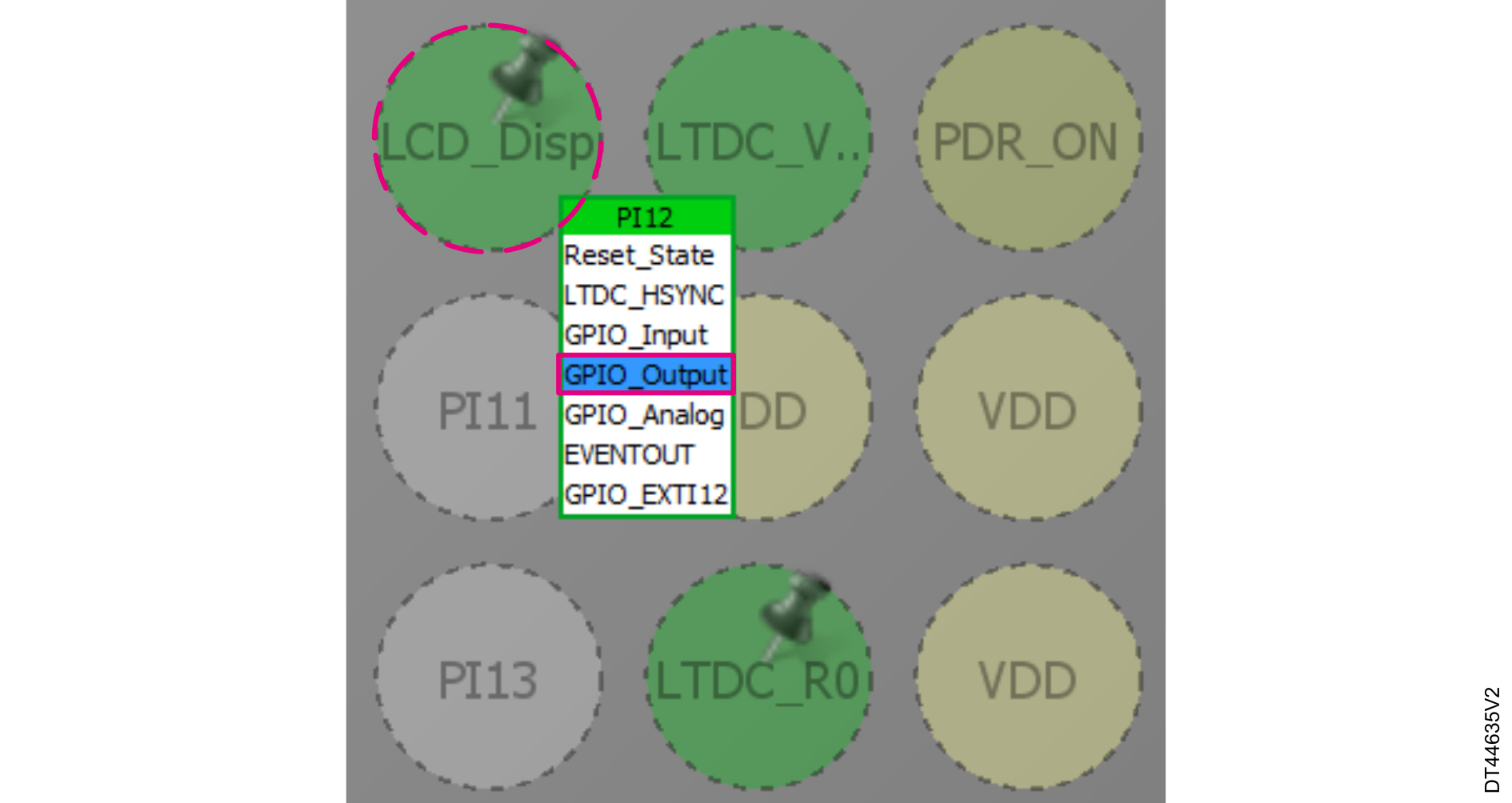
The LCD_DISP pin (PI12 pin) has to be configured as an output push-pull with high level in order to enable the display, otherwise the display stays in Standby mode.
To configure the LCD_DISP pin in output mode with STM32CubeMX, in the pinout tab click on the PI12 pin then select GPIO_Output (see Figure 41 STM32CubeMX: display enable pin (LCD_DISP) configuration).
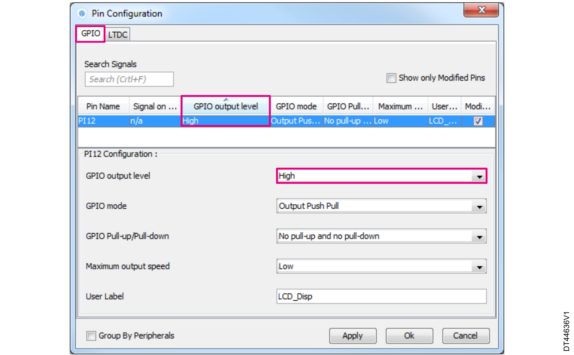
Then, the LDC_DISP (PI12) pin must be configured to high level: in the Configuration tab, click on the GPIO button. In the Pin Configuration window, set the GPIO output level to high as described in Figure 42 STM32CubeMX: setting LCD_DISP pin output level to high.
Due to the R85 pull-up resistance, the backlight is at its highest level by default if the LCD_BL_CTRL (PK3) pin is kept floating. There is no need to configure this pin.
The FIFO underrun and transfer error interrupts are enabled in the hal_ltdc driver HAL_LTDC_Init() function. The user must just enable the LTDC global interrupt on the NVIC side.
To enable the LTDC global interrupts using STM32CubeMX, select the Configuration tab then click on the LTDC button as shown in Figure 39 STM32CubeMX: LTDC configuration.
In the LTDC Configuration window shown in Figure 43 STM32CubeMX: enabling LTDC global and error interrupts, select the NVIC settings tab. Check the LTDC global interrupts then click on the OK button.
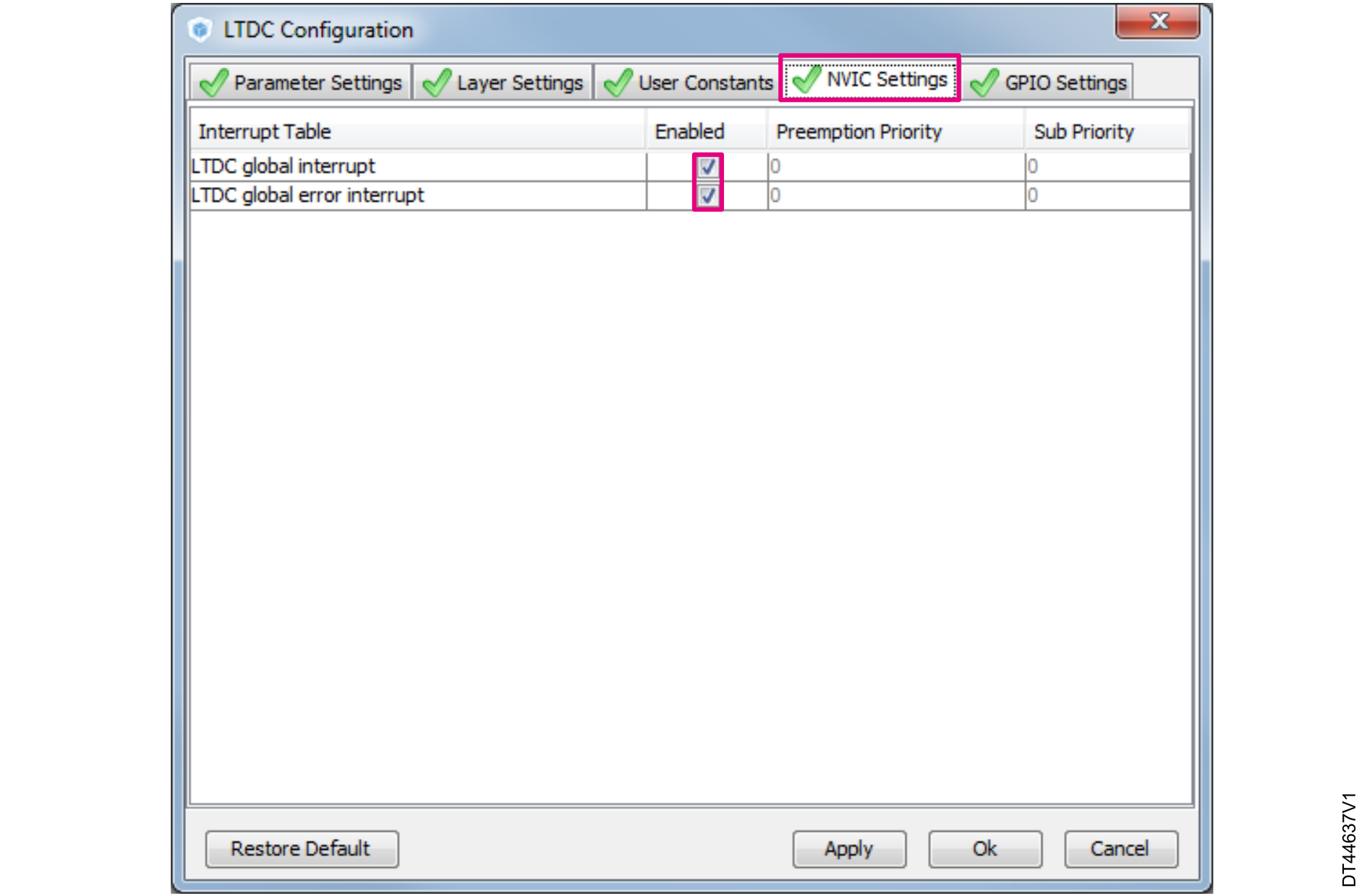
This section demonstrates how to configure LTDC clocks, timings, and layer parameters using STM32CubeMX.
System clock configuration
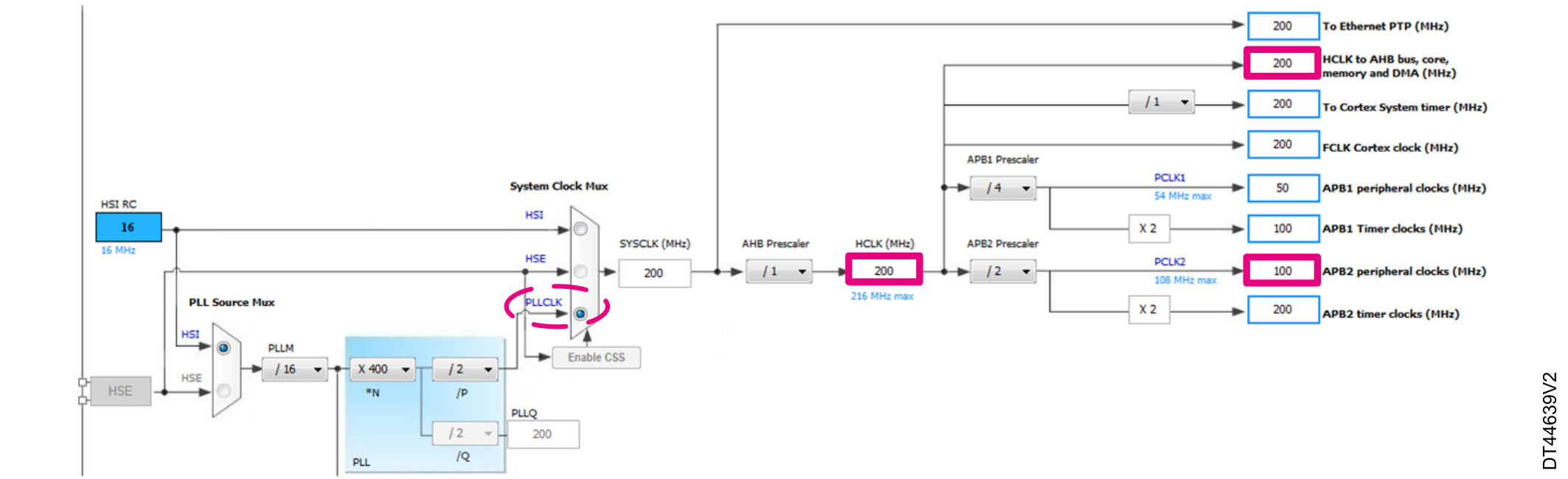
In this example the system clock is configured with the following configuration:
HCLK is set to 200 MHz but not 216 MHz. This is to set the SDRAM_FMC at its maximum speed of 100 MHz with HCLK/2 prescaler.
In order to configure the system clock using STM32CubeMX, select the Clock Configuration tab as shown in Figure 44 STM32CubeMX: clock configuration tab.
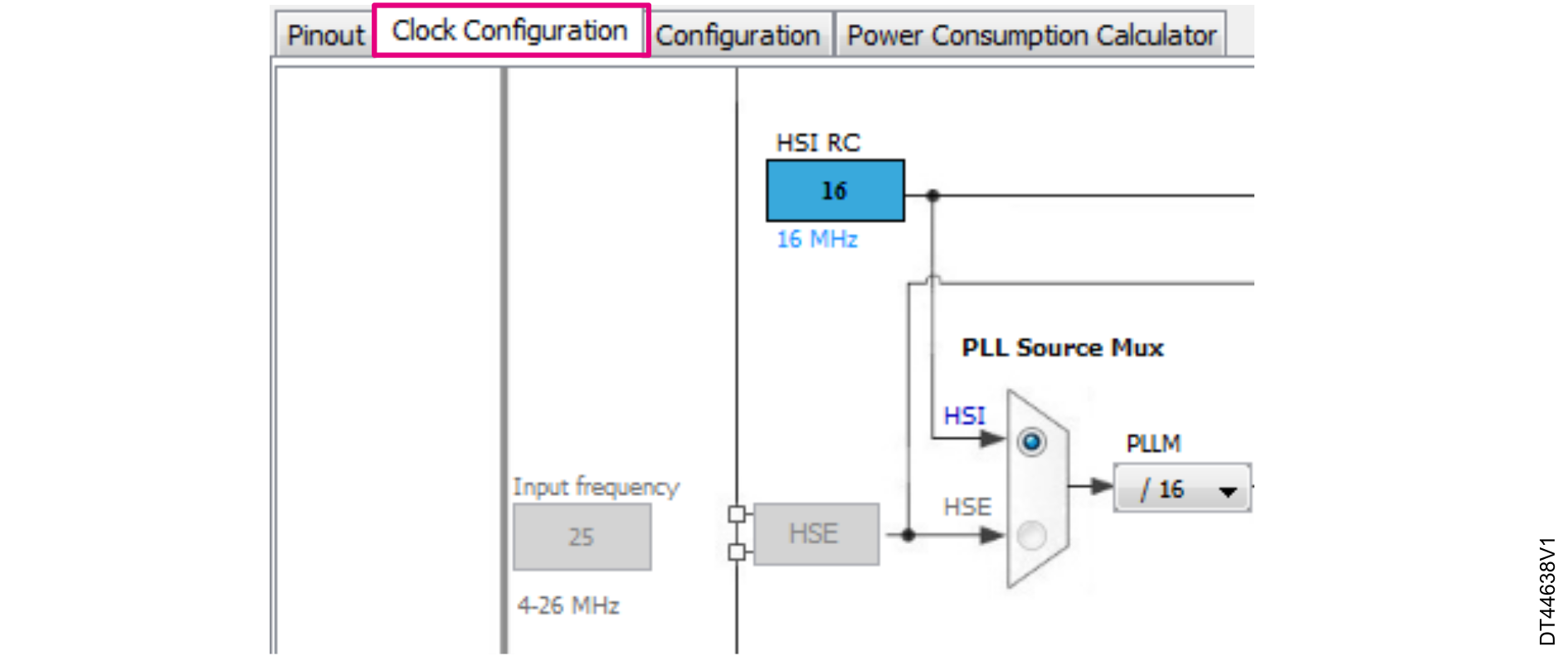
To get the system clock HCLK @ 200 MHz, set the PLLs and the prescalers in the Clock Configuration tab as shown in Figure 45 STM32CubeMX: System clock configuration.
Pixel clock configuration
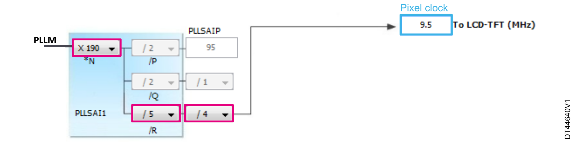
The LCD_CLK must be calculated using the parameters found in the display datasheet. In order to do the calculation, the user must determine the total width and total height. The pixel clock is calculated with a 60 Hz refresh rate as shown below:
LCD_CLK = TOTALW x TOTALH x refresh rate (see extracted display timing parameters in LTDC clocks and timings configuration)
==> LCD_CLK = 531 x 297 x 60 = 9.5 MHz
To configure the LTDC pixel clock to 9.5 MHz using STM32CubeMX, select the Clock Configuration tab, then set the PLLSAI and the prescalers as shown in Figure 46 STM32CubeMX: LTDC pixel clock configuration.
Timing parameter configuration
In order to configure the display timings using STM32CubeMX, the user must extract the timing parameters from the device datasheet. For this example, see an extract of ROCKTECH datasheet on Table 22 LCD-TFT timings extracted from ROCKTECH RK043FN48H datasheet. It is recommended to use the typical display timings.
In order to configure the display timing, the user must go to the Configuration tab as indicated in Figure 39 STM32CubeMX: LTDC configuration, and then click on the LTDC button. In the LTDC configuration window, the user must select the Parameter Settings tab and fill in the timing values (refer to Figure 47 STM32CubeMX: LTDC timing configuration).
LTDC control signals polarity configuration
Referring to the display datasheet, HSYNC and VSYNC must be active low and the DE signal must be active high. As the DE signal is inverted in the output, it must be set to active low as well. The LCD_CLK signal must not be inverted.
Figure 47 STM32CubeMX: LTDC timing configuration shows the control signal polarity configuration and the LTDC configuration according to the ROCKTECH display datasheet.
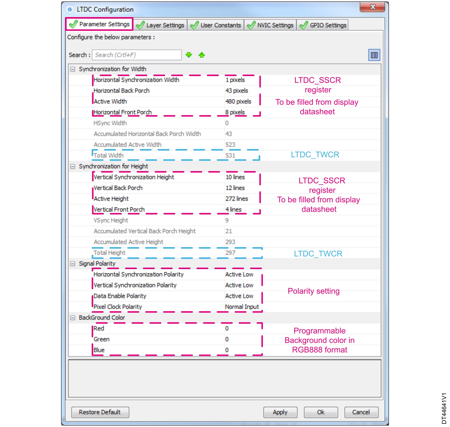
At this stage, all LTDC clocks and timings have been set in the STM32CubeMX project.
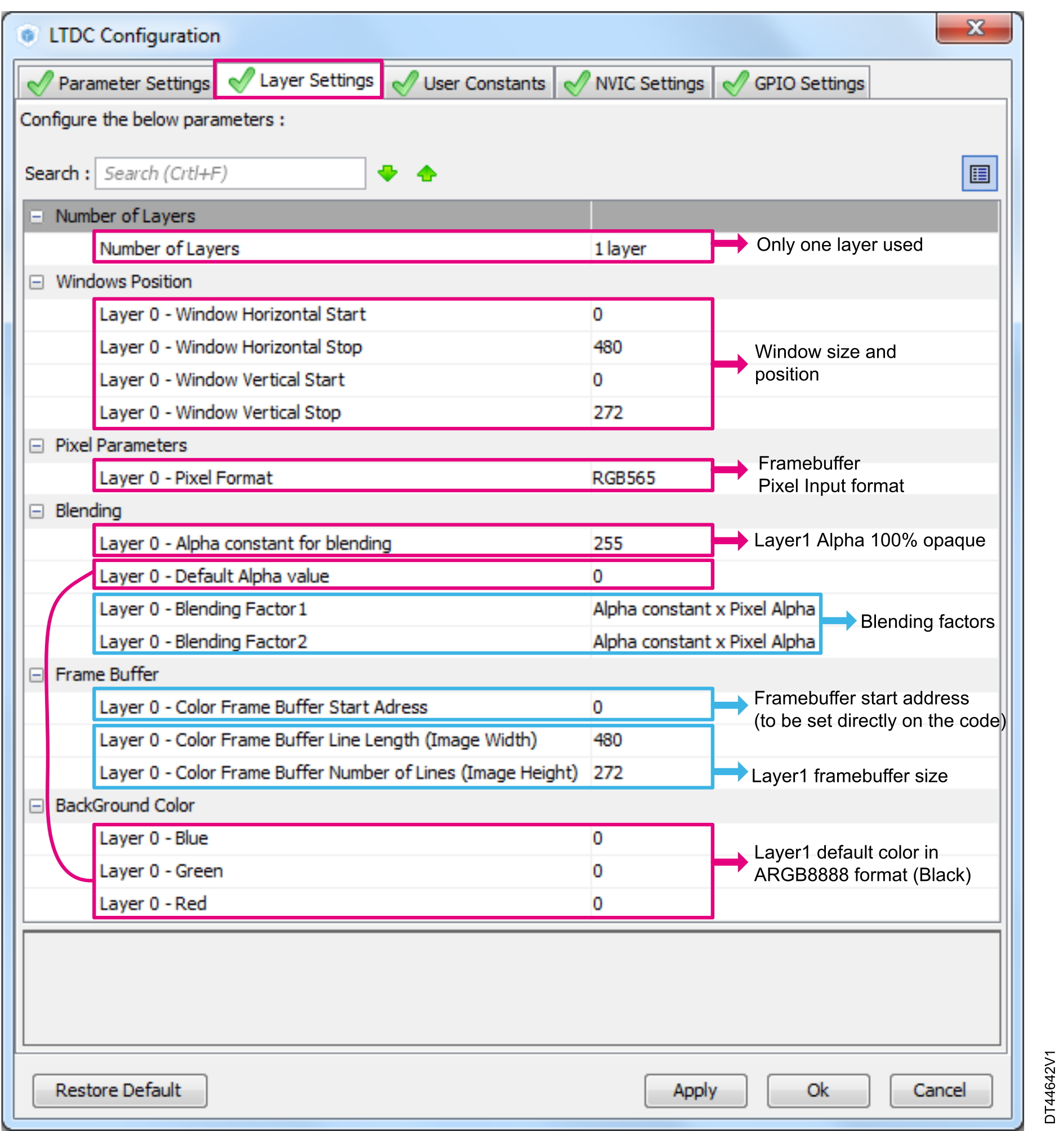
The user must configure the LTDC Layer1 parameters according to the display size and the color depth.
If needed, the user can also enable the Layer2 by setting to 2layers the Numberof Layers field in the LTDC configuration window shown in Figure 48 STM32CubeMX: LTDC Layer1 parameters setting.
To set the LTDC Layer1 parameters using STM32CubeMX, the user must select the Configuration tab then click on the LTDC button as shown in Figure 38 STM32CubeMX: PJ7 pin configuration to LTDC_G0 alternate function.
In the LTDCConfiguration window shown in Figure 48 STM32CubeMX: LTDC Layer1 parameters setting, the user must select the Layer Settings tab, set the LTDC layer1 parameters and then click on the OK button.
At this step, the user can generate the project with the desired toolchain by clicking on Project->Generate Code
In order to ensure that the LTDC is properly configured respecting the display panel specifications, it is important to display an image from the internal flash.
To do it, the user must first convert the image to a C or a header file and add it to the project.
The user must generate the header file respecting the configured LTDC layer pixel input format RGB565 (see Pixel input format and Storing graphic primitives).
In this example, the LCD-Image-Converter-20161012 tool is used (see Storing graphic primitives for more details on this tool).
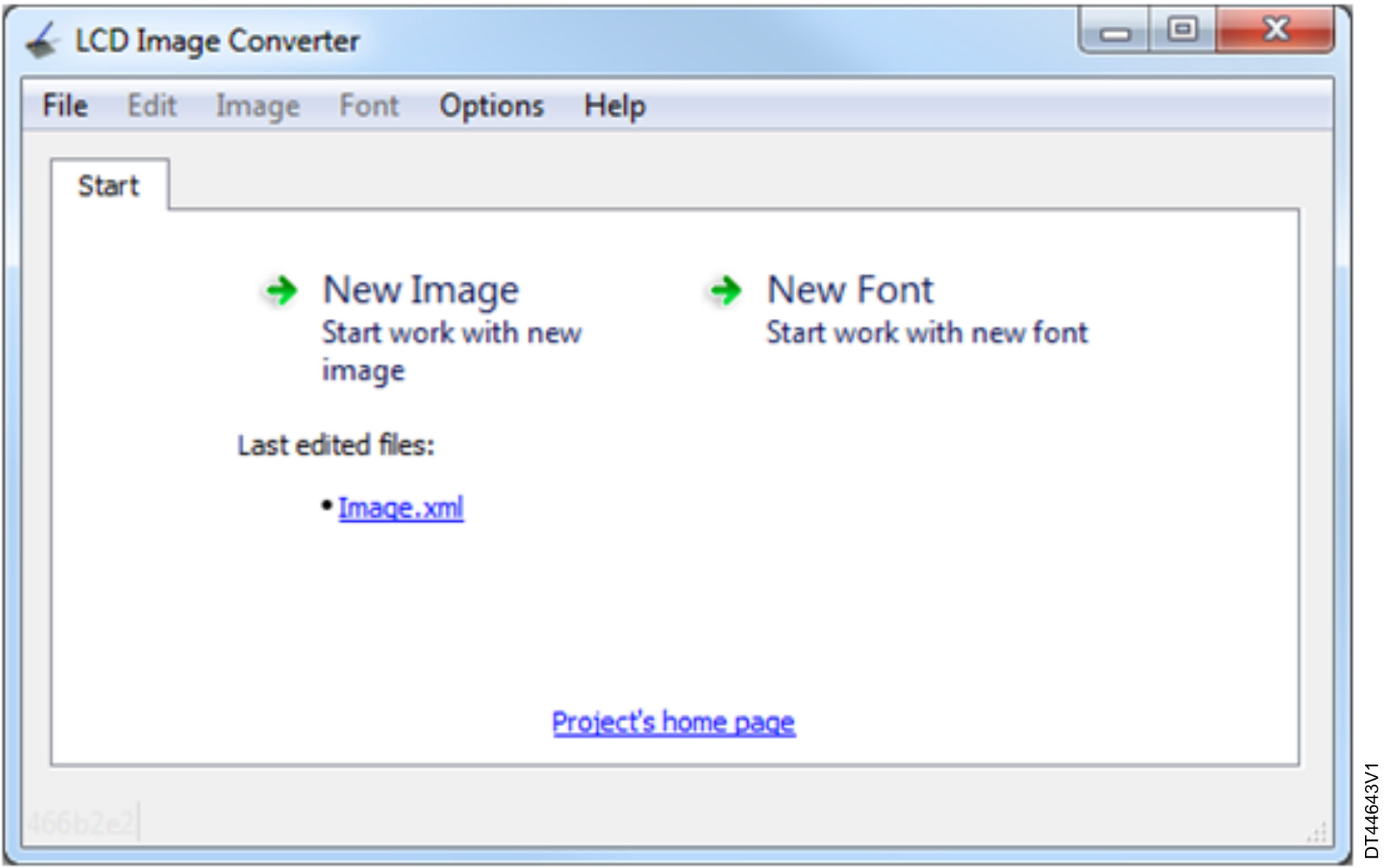
To convert an image, the user must first run the LCD-Image-Converter tool. Then, in the home page shown in Figure 49 LCD-Image-Converter: home page, click on File->Open and select the image file to be converted.
The used image size must be aligned with the LTDC Layer1 configuration (480 x 272). If the used image size is not aligned with the LTDC Layer1 configuration, the user can resize the image by going to Image->Resize or choose another image with the correct size.
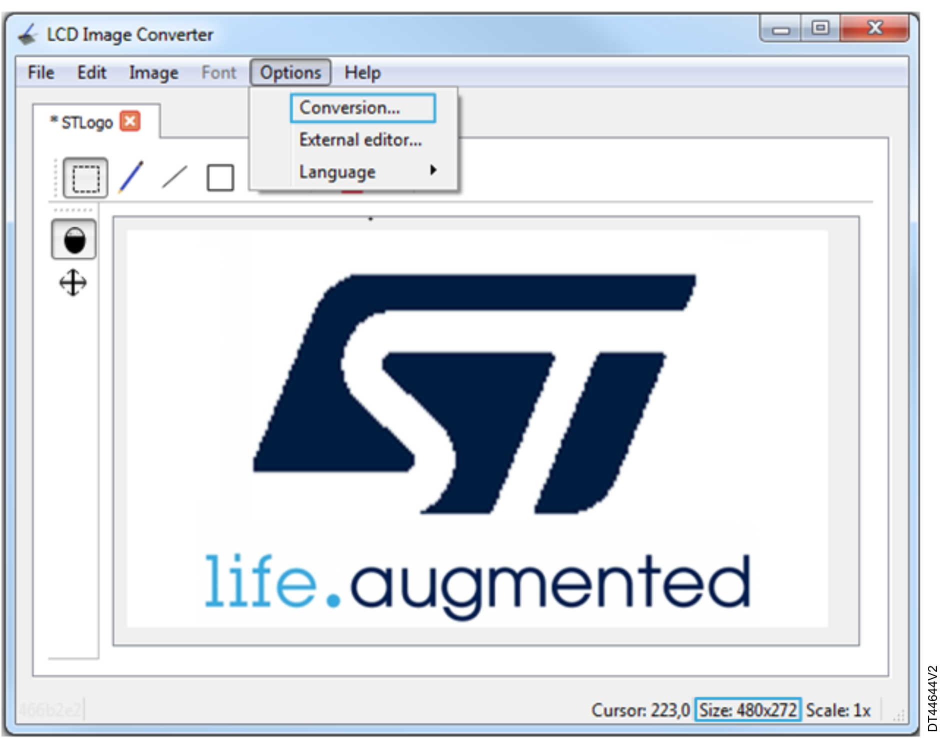
For this example, the used image size is 480 x 272 and shows the STMicroelectronics logo (see Figure 50 LCD-Image-Converter: image project).
The image is then displayed on the LCD-Image-Converter tool home page as described in Figure 50 LCD-Image-Converter: image project.
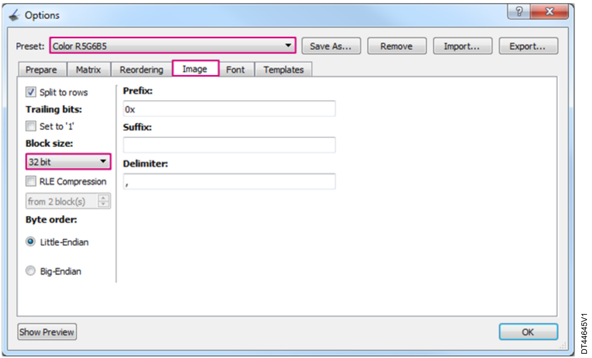
To convert the image to a header file avoiding the Red and Blue swap issue explained in Storing graphic primitives, the user must configure the tool to convert the image to a table of 32-bit words. To do it, in the home page menu, click on Options->Conversion as shown in Figure 50 LCD-Image-Converter: image project.
In the Options window shown in Figure 51 LCD-Image-Converter: setting conversion options, select the Image tab then select the RGB565 color in the Preset field. Set the Block size field to 32-bit and click on the OK button.
The user can also convert the image to a table of bytes, but in that case he must swap the Red and Blue colors in the Conversion window matrix tab.
To generate the header file, click on File->Convert. In the displayed window shown in Figure 52 LCD-Image-Converter: generating the header file, set the file type to C/C++ headers (*.h), then save the *.h file in include \Inc directory (same location as main.h file) by clicking on the Save button.
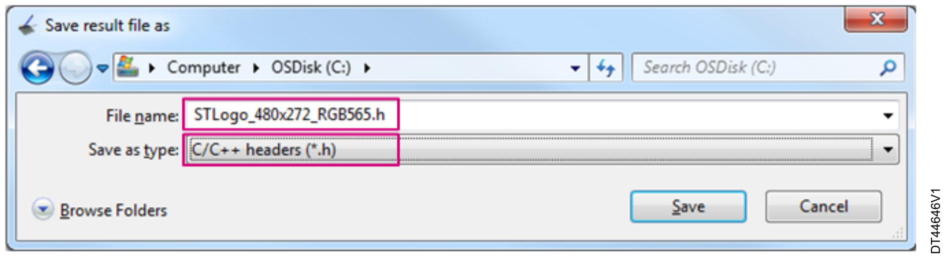
The generated header file must be included in the main.c file. It includes a table of 32-bit words where each word represents two pixels.
In this header file, the user must comment the structure definition located just after the table and keep only the table definition as shown below:
/* Converted image: image_data_STLogo definition */
const uint32_t image_data_STLogo[65280] = {0xffffffff, 0xffffffff, ........};The generated project by STM32CubeMX must include in the main.c file the MX_LTDC_Init() function that allows the LTDC peripheral configuration.
In order to display the image, the user must set the LTDC Layer1 framebuffer start address to the address of the image in the internal flash.
The MX_LTDC_Init() function is presented below with the framebuffer start address setting.
/* LTDC configuration function generated by STM32CubeMX tool */
static void MX_LTDC_Init(void)
{

    LTDC_LayerCfgTypeDef pLayerCfg;

    hltdc.Instance = LTDC;
    /* LTDC control signals polarity setting */
    hltdc.Init.HSPolarity = LTDC_HSPOLARITY_AL;
    hltdc.Init.VSPolarity = LTDC_VSPOLARITY_AL;
    hltdc.Init.DEPolarity = LTDC_DEPOLARITY_AL;
    hltdc.Init.PCPolarity = LTDC_PCPOLARITY_IPC;
    /* Timings configuration */
    hltdc.Init.HorizontalSync = 0;
    hltdc.Init.VerticalSync = 9;
    hltdc.Init.AccumulatedHBP = 43;
    hltdc.Init.AccumulatedVBP = 21;
    hltdc.Init.AccumulatedActiveW = 523;
    hltdc.Init.AccumulatedActiveH = 293;
    hltdc.Init.TotalWidth = 531;
    hltdc.Init.TotalHeigh = 297;
    /* Background color */
    hltdc.Init.Backcolor.Blue = 0;
    hltdc.Init.Backcolor.Green = 0;
    hltdc.Init.Backcolor.Red = 0x0;
    if (HAL_LTDC_Init(&hltdc) != HAL_OK)
    {
        Error_Handler();
    }
    /* Layer1 Window size and position setting */
    pLayerCfg.WindowX0 = 0;
    pLayerCfg.WindowX1 = 480;
    pLayerCfg.WindowY0 = 0;
    pLayerCfg.WindowY1 = 272;
    /* Layer1 Pixel Input Format setting */
    pLayerCfg.PixelFormat = LTDC_PIXEL_FORMAT_RGB565;
    /* Layer1 constant Alpha setting 100% opaque */
    pLayerCfg.Alpha = 255;
    /* Layer1 Blending factors setting */
    pLayerCfg.BlendingFactor1 = LTDC_BLENDING_FACTOR1_PAxCA;
    pLayerCfg.BlendingFactor2 = LTDC_BLENDING_FACTOR2_PAxCA;
    /* User should set the framebuffer start address (can be 0xC0000000 if external SDRAM is used)*/
    pLayerCfg.FBStartAdress = (uint32_t)&image_data_STLogo;
    pLayerCfg.ImageWidth = 480;
    pLayerCfg.ImageHeight = 272;
    /* Layer1 Default color setting */
    pLayerCfg.Alpha0 = 0;
    pLayerCfg.Backcolor.Blue = 0;
    pLayerCfg.Backcolor.Green = 0;
    pLayerCfg.Backcolor.Red = 0;
    if (HAL_LTDC_ConfigLayer(&hltdc, &pLayerCfg, 0) != HAL_OK)
    {
        Error_Handler();
    }
}
Once the LTDC is correctly configured in the project, the user must build the project, and then run it.
The external SDRAM must be configured as it contains the LTDC framebuffer. To configure the FMC_SDRAM and the SDRAM memory device mounted on the STM32746G-Discovery board, STM32CubeMX or the existing BSP driver can be used.
To configure the FMC_SDRAM using the BSP driver, follow the steps below:
BSP_SDRAM_Init() function in the main() function.As illustrated in Special recommendations for Cortex M7 (STM32F7/H7) and Cortex M55 (STM32N6), the MPU attributes must be correctly configured to prevent graphical performance issues related to the Cortex-M7 speculative read accesses and cache maintenance.
This section describes an example of MPU attribute configuration with respect to the STM32F746G-DISCO board hardware configuration.
The MPU memory attributes can be easily configured with STM32CubeMX. A code example of MPU configuration generated using STM32CubeMX is described at the end of this section.
In this configuration example, the double-framebuffer technique is used. The frontbuffer is placed in the SDRAM Bank1 while the backbuffer is placed in the SDRAM Bank2 with respect to the SDRAM bandwidth optimization described in Optimizing the LTDC framebuffer fetching from SDRAM.
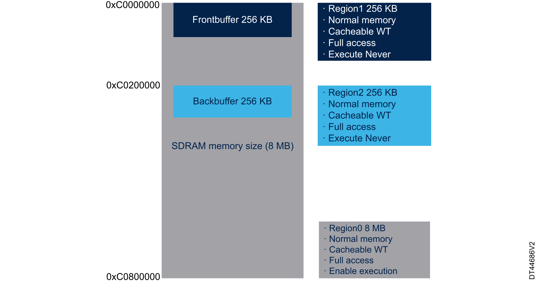
This example shows how to configure the MPU for the Quad-SPI interface. The Quad-SPI memory contains graphic primitives and can be accessed by Cortex-M7, DMA2D, or LTDC. For that, the Quad-SPI interface must be set to Memory-mapped mode and the MPU regions must be configured as described below:
Figure 54 MPU configuration for Quad-SPI region illustrates the MPU configuration of the Quad-SPI region.
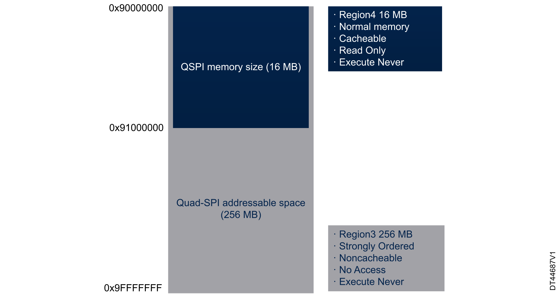
The following code (generated by STM32CubeMX) shows how to set the MPU attributes for the FMC_SDRAM and Quad-SPI respecting the previously described configurations.
/* MPU Configuration */
void MPU_Config(void)
{
    MPU_Region_InitTypeDef MPU_InitStruct;

    /* Disables the MPU */
    HAL_MPU_Disable();
    /* Configure the MPU attributes for region 0 */
/* Configure the MPU attributes for SDRAM to normal memory*/
    MPU_InitStruct.Enable = MPU_REGION_ENABLE;
    MPU_InitStruct.Number = MPU_REGION_NUMBER0;
    MPU_InitStruct.BaseAddress = 0xC0000000;
    MPU_InitStruct.Size = MPU_REGION_SIZE_8MB;
    MPU_InitStruct.SubRegionDisable = 0x0;
    MPU_InitStruct.TypeExtField = MPU_TEX_LEVEL0;
    MPU_InitStruct.AccessPermission = MPU_REGION_FULL_ACCESS;
    MPU_InitStruct.DisableExec = MPU_INSTRUCTION_ACCESS_ENABLE;
    MPU_InitStruct.IsShareable = MPU_ACCESS_NOT_SHAREABLE;
    MPU_InitStruct.IsCacheable = MPU_ACCESS_CACHEABLE;
    MPU_InitStruct.IsBufferable = MPU_ACCESS_NOT_BUFFERABLE;

    HAL_MPU_ConfigRegion(&MPU_InitStruct);

    /* Configure the MPU attributes for region 1 */
/* Configure the MPU attributes for the frontbuffer to normal memory*/
    MPU_InitStruct.Enable = MPU_REGION_ENABLE;
    MPU_InitStruct.Number = MPU_REGION_NUMBER1;
    MPU_InitStruct.BaseAddress = 0xC0000000;
    MPU_InitStruct.Size = MPU_REGION_SIZE_256KB;
    MPU_InitStruct.SubRegionDisable = 0x0;
    MPU_InitStruct.TypeExtField = MPU_TEX_LEVEL0;
    MPU_InitStruct.AccessPermission = MPU_REGION_FULL_ACCESS;
    MPU_InitStruct.DisableExec = MPU_INSTRUCTION_ACCESS_DISABLE;
    MPU_InitStruct.IsShareable = MPU_ACCESS_NOT_SHAREABLE;
    MPU_InitStruct.IsCacheable = MPU_ACCESS_CACHEABLE;
    MPU_InitStruct.IsBufferable = MPU_ACCESS_NOT_BUFFERABLE;

    HAL_MPU_ConfigRegion(&MPU_InitStruct);

    /* Configure the MPU attributes for region 2 */
/* Configure the MPU attributes for the backbuffer to normal memory*/
    MPU_InitStruct.Enable = MPU_REGION_ENABLE;
    MPU_InitStruct.Number = MPU_REGION_NUMBER2;
    MPU_InitStruct.BaseAddress = 0xC0200000;
    MPU_InitStruct.Size = MPU_REGION_SIZE_256KB;
    MPU_InitStruct.SubRegionDisable = 0x0;
    MPU_InitStruct.TypeExtField = MPU_TEX_LEVEL0;
    MPU_InitStruct.AccessPermission = MPU_REGION_FULL_ACCESS;
    MPU_InitStruct.DisableExec = MPU_INSTRUCTION_ACCESS_DISABLE;
    MPU_InitStruct.IsShareable = MPU_ACCESS_NOT_SHAREABLE;
    MPU_InitStruct.IsCacheable = MPU_ACCESS_CACHEABLE;
    MPU_InitStruct.IsBufferable = MPU_ACCESS_NOT_BUFFERABLE;

    HAL_MPU_ConfigRegion(&MPU_InitStruct);

/* Configure the MPU attributes for region 3 */
/* Configure the MPU attributes for Quad-SPI area to strongly ordered memory*/
    MPU_InitStruct.Enable = MPU_REGION_ENABLE;
    MPU_InitStruct.Number = MPU_REGION_NUMBER3;
    MPU_InitStruct.BaseAddress = 0x90000000;
    MPU_InitStruct.Size = MPU_REGION_SIZE_256MB;
    MPU_InitStruct.SubRegionDisable = 0x0;
    MPU_InitStruct.TypeExtField = MPU_TEX_LEVEL0;
    MPU_InitStruct.AccessPermission = MPU_REGION_NO_ACCESS;
    MPU_InitStruct.DisableExec = MPU_INSTRUCTION_ACCESS_DISABLE;
    MPU_InitStruct.IsShareable = MPU_ACCESS_NOT_SHAREABLE;
    MPU_InitStruct.IsCacheable = MPU_ACCESS_NOT_CACHEABLE;
    MPU_InitStruct.IsBufferable = MPU_ACCESS_NOT_BUFFERABLE;

    HAL_MPU_ConfigRegion(&MPU_InitStruct);

/* Configure the MPU attributes for region 4 */
/* Configure the MPU attributes for QSPI memory to normal memory*/
    MPU_InitStruct.Enable = MPU_REGION_ENABLE;
    MPU_InitStruct.Number = MPU_REGION_NUMBER4;
    MPU_InitStruct.BaseAddress = 0x90000000;
    MPU_InitStruct.Size = MPU_REGION_SIZE_16MB;
    MPU_InitStruct.SubRegionDisable = 0x0;
    MPU_InitStruct.TypeExtField = MPU_TEX_LEVEL0;
    MPU_InitStruct.AccessPermission = MPU_REGION_PRIV_RO;
    MPU_InitStruct.DisableExec = MPU_INSTRUCTION_ACCESS_DISABLE;
    MPU_InitStruct.IsShareable = MPU_ACCESS_NOT_SHAREABLE;
    MPU_InitStruct.IsCacheable = MPU_ACCESS_CACHEABLE;
    MPU_InitStruct.IsBufferable = MPU_ACCESS_NOT_BUFFERABLE;

    HAL_MPU_ConfigRegion(&MPU_InitStruct);

    /* Enables the MPU */
    HAL_MPU_Enable(MPU_PRIVILEGED_DEFAULT);
}