DMA2D usage
The DMA2D is a master on the AHB/AXI bus matrix performing graphical data transfers inter-memories. It is recommended to use the DMA2D in order to offload the CPU.
The DMA2D implements four basic tasks:
- Fill a rectangular shape with a unique color.
- Copy a frame or a rectangular part of a frame from a memory to another.
- Convert the pixel format of a frame or a rectangular part of a frame while transferring it from one memory to another memory.
- Blend two images with different sizes and pixel format and store the resulting image in one resulting memory.
LTDC and DMA2D/CPU synchronization
When only one framebuffer is used, there is a risk that the framebuffer computation is displayed on the screen. Multiple buffering techniques, such as the double buffering, are commonly used to avoid displaying the framebuffer calculation on the screen.
Even when using a double-buffering technique, a tearing effect may appear due to a nonsynchronization between the LTDC and the framebuffer update (either by the CPU or the DMA2D). A way to solve this issue is the use of the VSYNC signal to synchronize the workflow of these two masters (LTDC and either CPU or DMA2D).
The LTDC fetches the graphical data from a buffer (called frontbuffer) while the DMA2D prepares the next frame in another buffer (called backbuffer). The VSYNC period indicates the end of the actual frame display and that the two buffers needs to be flipped.
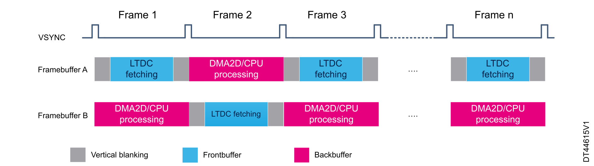
The LTDC provides different options to synchronize this workflow:
- Program the line interruption with the value of the last screen line. The interrupt handler must flip the framebuffers and start the next framebuffer calculation.
- Program the shadow reload register (LTDC_SRCR) to vertical blanking reload to change the LTDC framebuffer address on the VSYNC period, and poll on VSYNC bit of the LTDC_CDSR register to unblock the DMA2D.
Graphic performance optimization
As previously stated in this document, the framebuffer memory bandwidth is the most important parameter for a graphic application. This section provides some recommendations to optimize the graphic performances based on bandwidth optimizations of the framebuffer memory.
Memory allocation
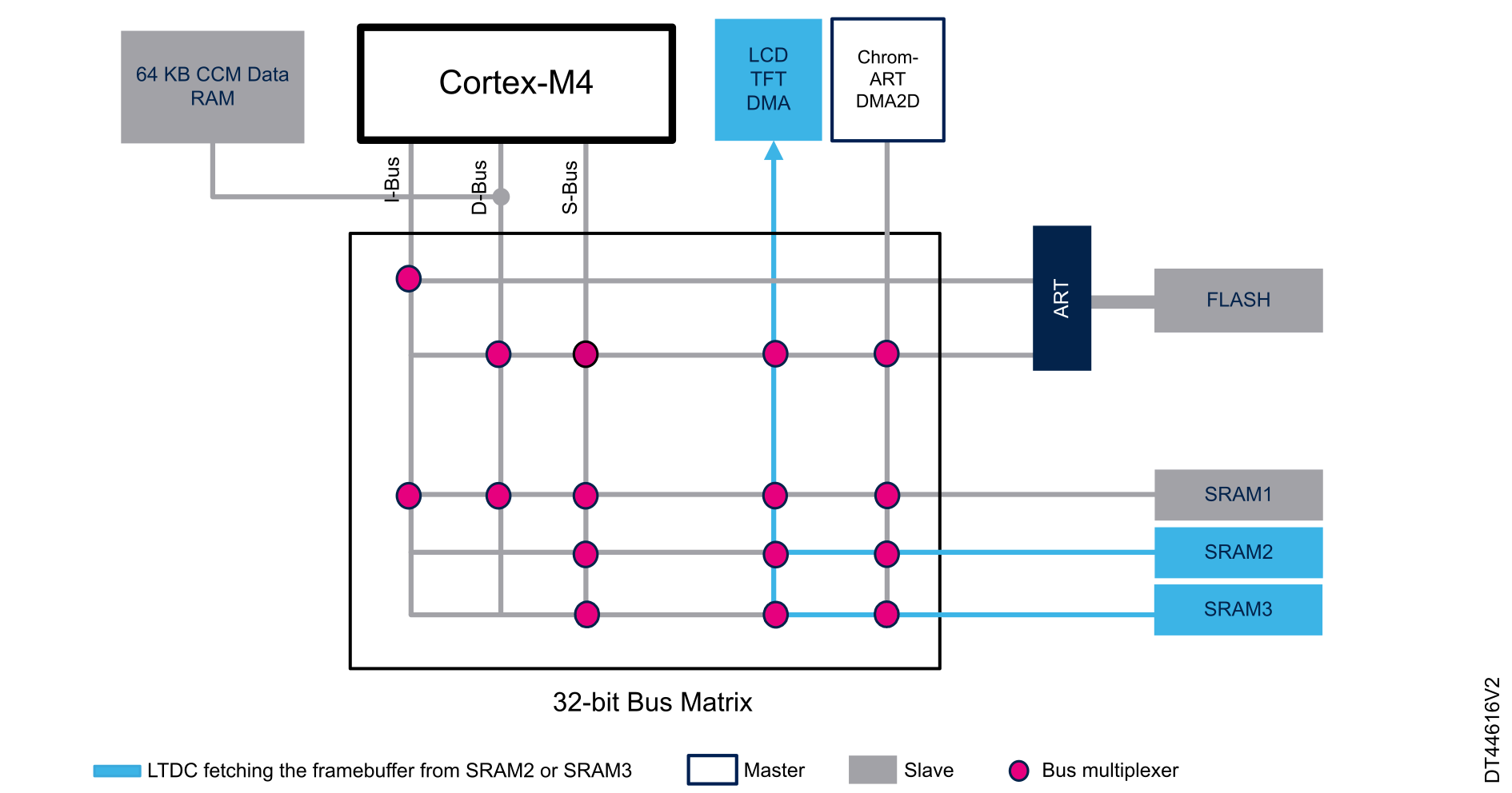
The smart architecture of the STM32 MCUs enables a significant system performance gain when using the internal SRAM memory, split into two or more slaves.
Splitting up the slaves memories between masters helps to decrease the competition between them when they access simultaneously the same SRAM. This action also creates an additional system bus bandwidth.
As shown in the example described in Figure 25 Example of taking advantage from memory slaves split on STM32F4x9, SRAM2 and SRAM3 are dedicated to graphics for the framebuffer while the SRAM1 is used by the CPU.
Optimizing the LTDC framebuffer fetching from external memories (SDRAM or SRAM)
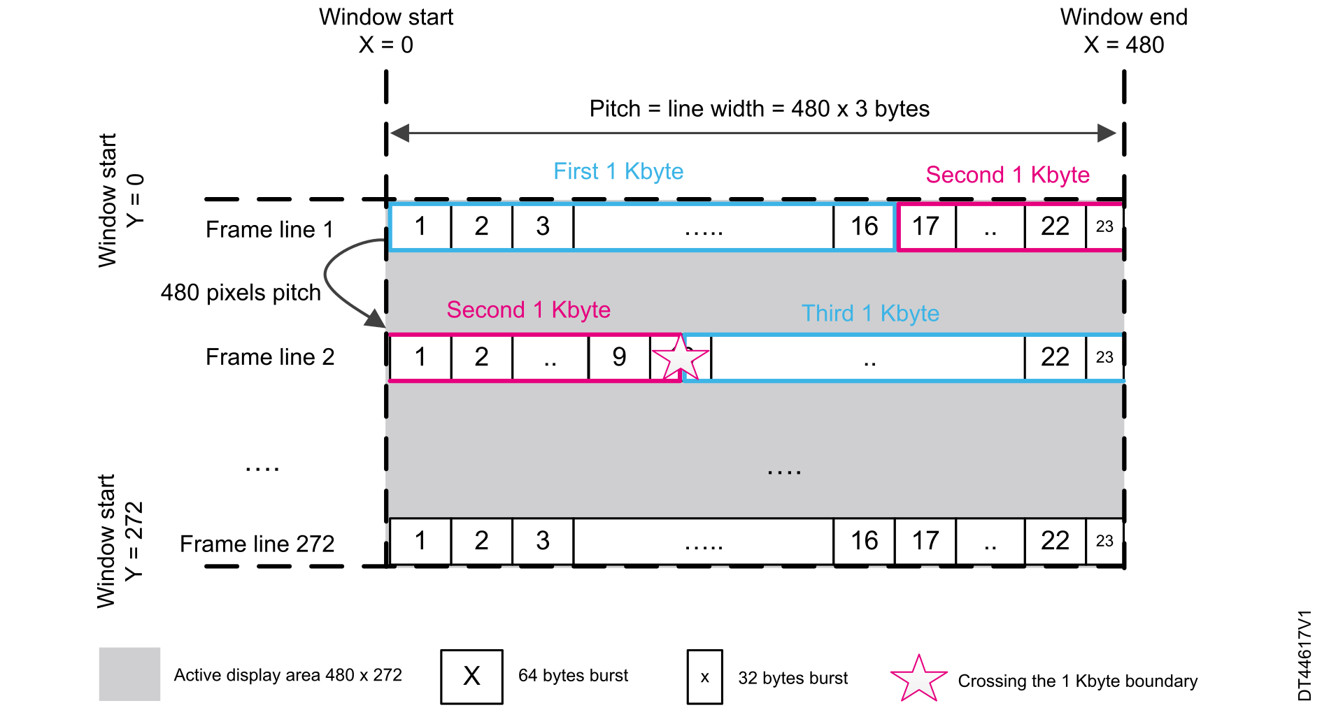
Another consideration related to the SDRAM/SRAM is the placement of the framebuffer and the line length data size. Since the AHB bus matrix prohibits a memory burst access that crosses the 1-Kbyte boundary, and as the LTDC performs burst read of 64 bytes (for AHB), placing the content of the framebuffer in an address at the edge of 1 Kbyte splits the burst read into single accesses, which can heavily affect the graphical performances.
The same problem can occur when the data size of one line of pixels is not a multiple of 64 bytes (for AHB). Under these conditions and after a number of accesses, the LTDC read burst crosses the 1-Kbyte boundary that splits the burst read into single accesses.
As a consequence, when the LTDC does not generate a burst, each access is interrupted by a CPU or another master access (such as Chrom-Art Accelerator or Ethernet).
These interruptions highly reduce the LTDC bandwidth on a high-latency memory like the external SDRAM that leads to an underrun.
To solve the issue described above, the user may choose a color depth that does not lead to the described issue, or use one of the two following methods:
- Reduce the layer window and the framebuffer line widths.
- Add a number of dummy bytes at the end of every line of pixels to match the closest frame line width multiple of 64 bytes (for AHB).
Example: 480 x 272 display with 24 bpp
For a 480 x 272 display (the frame line width is 480 pixels) and with a 24 bpp color depth, the line width size is equal to 1440 bytes that is not a multiple of 64 bytes (for AHB).
Note:
For that resolution, to have a multiple line width size of 64 bytes (for AHB), the user can use another color depth such as RGB565.
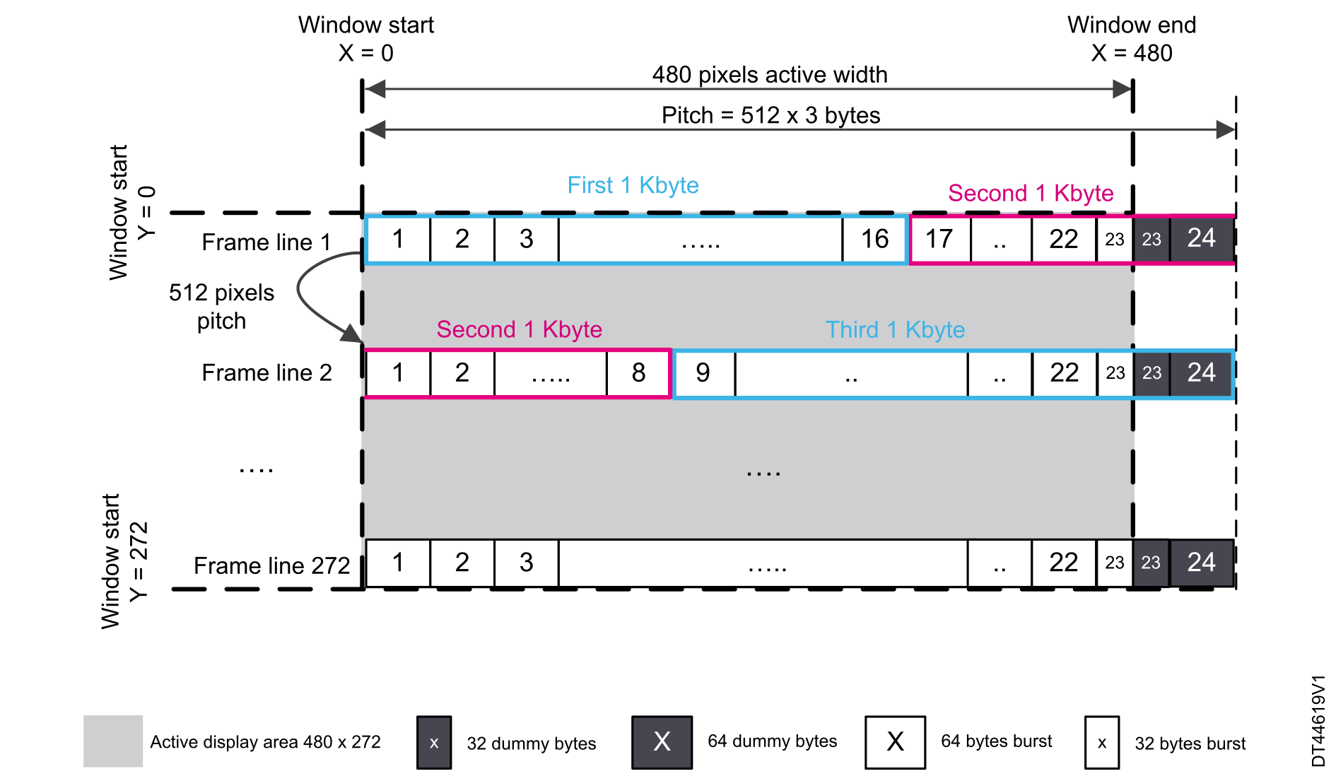
Since the frame line is composed of 22 bursts of 64 bytes (for AHB) and one 32 bytes burst, the 10th burst of the second line of the frame crosses the 1-Kbyte boundary. This leads to the split of the read operation into single accesses.
Figure 26 Burst access crossing the 1-Kbyte boundary illustrates the 1-Kbyte boundary cross problem for the given example.
For this example, the two methods to solve the crossing 1-Kbyte boundary issue are detailed below:
- First method
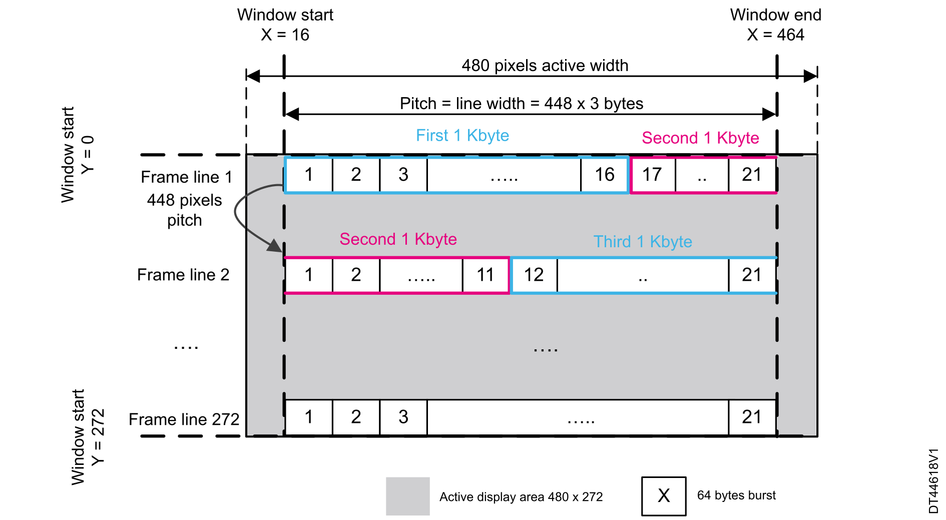
Reduce the layer window and the framebuffer line widths: use the LTDC layer windowing feature by reducing the window size to match the closest frame line width multiple of 64 bytes (for AHB).
Since the window width is reduced, the framebuffer size must also be reduced since the extra 22 and 23 bursts for all frame lines are not fetched nor displayed by LTDC.
This method solves the 1-Kbyte boundary crossing issue with a slight window width decrease (see Figure 27 Reducing layer window and framebuffer line widths).
The code below is based on the HAL drivers and shows an example of setting the pitch as described in Figure 27 Reducing layer window and framebuffer line widths:
/* Setting the Layer1 window to 448x272 at positions X = 16 and Y = 0 */
    pLayerCfg.WindowX0 = 16;
    pLayerCfg.WindowX1 = 464;
    pLayerCfg.WindowY0 = 0;
    pLayerCfg.WindowY1 = 272;
    pLayerCfg.PixelFormat = LTDC_PIXEL_FORMAT_RGB888;
    pLayerCfg.Alpha = 255;
    pLayerCfg.Alpha0 = 0;
    pLayerCfg.BlendingFactor1 = LTDC_BLENDING_FACTOR1_PAxCA;
    pLayerCfg.BlendingFactor2 = LTDC_BLENDING_FACTOR1_PAxCA;
/* Framebuffer start address: LTDC fetches the image directly from internal flash that the real image width is 448 pixels. Only the 448 pixels width is displayed*/
    pLayerCfg.FBStartAdress = (uint32_t)&image_data_Image_RGB888_448x272;
    pLayerCfg.ImageWidth = 448;
    pLayerCfg.ImageHeight = 272;
    pLayerCfg.Backcolor.Blue = 0;
    pLayerCfg.Backcolor.Green = 0;
    pLayerCfg.Backcolor.Red = 0;
    if (HAL_LTDC_ConfigLayer(&hltdc, &pLayerCfg, 0) != HAL_OK)
    {
        Error_Handler();
    }
- Second method
Add a number of dummy bytes at the end of every line of pixels to match the closest frame line width multiple of 64 bytes (for AHB). This can be done using the LTDC layer pitch (see Two programmable LTDC layers). To do this, the user must consider the two points below:
- The framebuffer must contain the dummy bytes (as described in Figure 28 Adding dummy bytes to make the line width multiple of 64 bytes):when writing data into the framebuffer, it can be done by programming an output offset of the DMA2D equal to the difference between the closest burst multiple and the actual line length data size.
- The LTDC line length must always be equal to the active data size, but, the LTDC pitch must be programmed with the value of the closest bytes number multiple of 64 bytes (for AHB).
The
HAL_LTDC_SetPitchfunction provided under the hal_ltdc driver can be used to program the desired pitch value in number of pixels. For the previous example, the value of the pitch to pass to this function must be equal to 512 (512 is the number of pixels per line corresponding to a line length size of 1536 bytes that is multiple of 64 bytes (for AHB).The code below is based on the HAL drivers and shows an example of setting the pitch as described in Figure 28 Adding dummy bytes to make the line width multiple of 64 bytes:
/* Setting the Layer1 window to 480x272 at positions X = 0 and Y = 0 */
    pLayerCfg.WindowX0 = 0;
    pLayerCfg.WindowX1 = 480;
    pLayerCfg.WindowY0 = 0;
    pLayerCfg.WindowY1 = 272;
    pLayerCfg.PixelFormat = LTDC_PIXEL_FORMAT_RGB888;
    pLayerCfg.Alpha = 255;
    pLayerCfg.Alpha0 = 0;
    pLayerCfg.BlendingFactor1 = LTDC_BLENDING_FACTOR1_PAxCA;
    pLayerCfg.BlendingFactor2 = LTDC_BLENDING_FACTOR1_PAxCA;
/* Framebuffer start address: LTDC fetches the image directly from internal flash that the real image width is 480 pixels but additional 32 pixels are added to each line to get a 512 pixels pitch.
Only the 480 pixels width is displayed*/
    pLayerCfg.FBStartAdress = (uint32_t)&image_data_Image_RGB888_512x272;
    pLayerCfg.ImageWidth = 480;
    pLayerCfg.ImageHeight = 272;
    pLayerCfg.Backcolor.Blue = 0;
    pLayerCfg.Backcolor.Green = 0;
    pLayerCfg.Backcolor.Red = 0;
    if (HAL_LTDC_ConfigLayer(&hltdc, &pLayerCfg, 0) != HAL_OK)
    {
        Error_Handler();
    }
/* Sets the Layer1 (index 0 refers to Layer1) Pitch to 512 pixels */
    HAL_LTDC_SetPitch(&hltdc, 512, 0);
Optimizing the LTDC framebuffer fetching from SDRAM
Making random access into a bank generates some precharge cycles that increase the SDRAM latency seen by the LTDC. As the LTDC performs sequential accesses, it is important that no other masters access the same SDRAM bank.
The external SDRAM is composed of multiple banks. Given that, making random accesses on a bank generates some precharge and activates some cycles. The framebuffer must be placed in an independent bank accessed only by the LTDC. This action reduces the external memory latency and leads to a higher throughput. As a consequence, when the double-framebuffer technique is used, it is recommended to have these buffers in two separate banks.
This can be done by storing the frontbuffer in the first address of the SDRAM and addressing the backbuffer by adding an offset with the size of one bank.
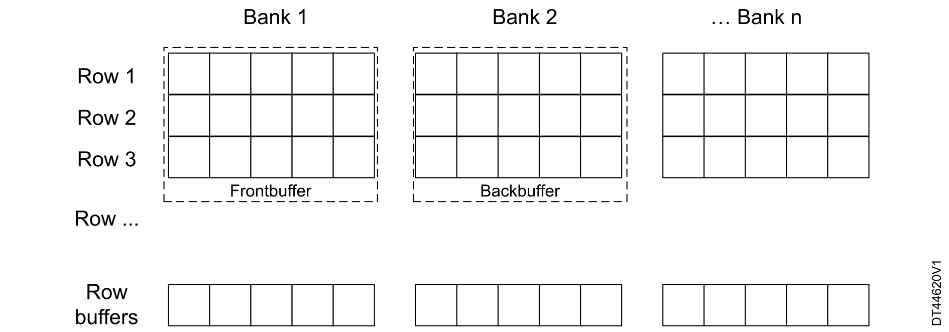
For instance, when the SDRAM bank size is equal to 4 Mbytes, the following line code can be used:
/* Framebuffer addresses within external SDRAM */
/* Frontbuffer in bank 1 of SDRAM memory */
uint32_t FrontBuffer = LCD_FB_START_ADRESS;
/* Backbuffer in the bank 2 of SDRAM memory */
uint32_t BackBuffer = LCD_FB_START_ADRESS + 1024 * 1024 * 4;
SDRAMRBURST
Another interesting feature allowing optimization of reading performances from the SDRAM is the use of RBURST.
The SDRAM controller adds a cacheable read FIFO with a depth of six 32-bit lines. The read FIFO is used when the read burst is enabled and allows the next read accesses to be anticipated during CAS latencies.
Framebuffer content update during blanking period
A way to optimize graphic performance (especially when the performance bottleneck is the framebuffer memory bandwidth), is to update the framebuffer content during the blanking period. Since, in this period, the LTDC does not fetch any pixel data from the framebuffer, the bus bandwidth is relaxed and the framebuffer update can be performed.