AN4861 · Application noteIntroduction to LCD-TFT display controller (LTDC) on STM32 MCUs
Download .pdfOpen in the full document

Two programmable LTDC layers

Two programmable LTDC layers

The LTDC features two layers, and each layer can be enabled, disabled, and configured separately. The order of the layer display is fixed, so it is always bottom-up. If two layers are enabled, the Layer2 is the top displayed window.

The LTDC features configurable blending factors. Blending is always active using an alpha value. The blending order is fixed and it is always bottom-up. If two layers are enabled, first the Layer1 is blended with the background color, and then the Layer2 is blended with the result of the blended color of Layer1 and the background.

The background color is programmable through the LTDC_BCCR register. A constant background color can be programmed in the RGB888 format where the BCRED[7:0] field is used for the red value, the BCGREEN[7:0] is used for the green value and the BCBLUE[7:0] is used for the blue value.

Figure 17 Blending two layers with a background illustrates the blending of two layers with a background.
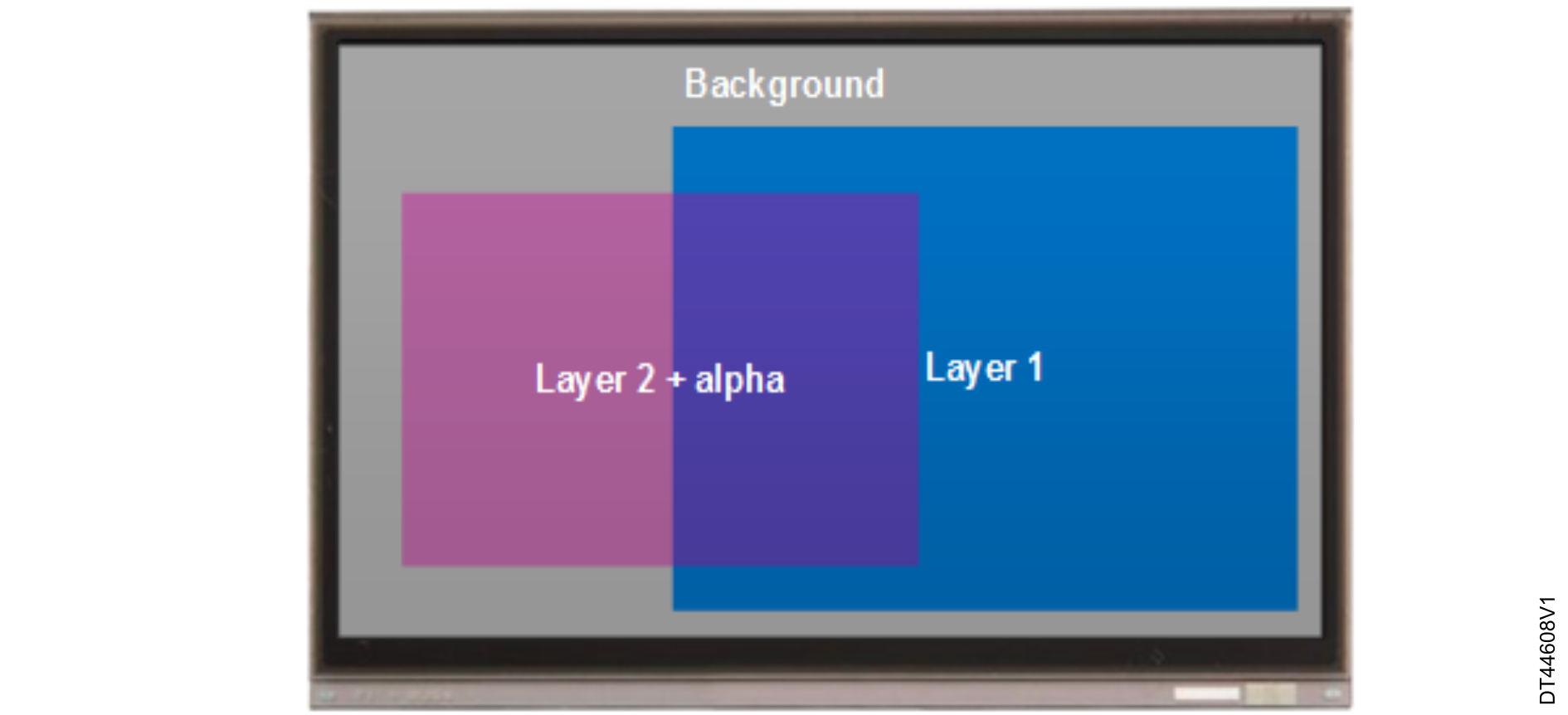
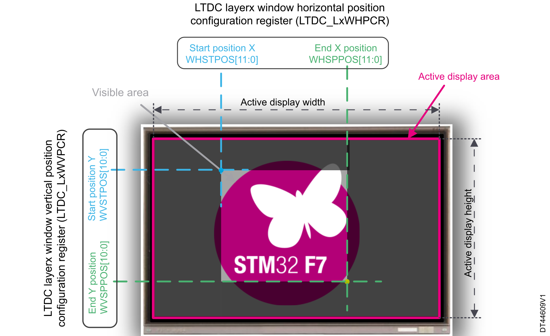
Figure 17. Blending two layers with a background


Flexible window position and size configuration

Every layer can be positioned and resized at runtime and it must be inside the active display area. The programmable layer position and size define the first and last visible pixel of a line and the first and last visible line in the window. It allows the display of either the full image (all the active display area) or only a part of the image frame.

Figure 18 Layer window programmable size and position. LTDC_LxWHPCR and LTDC_LxWVPCR are respectively LTDC layer x window horizontal and vertical position configuration registers where “x” can refer to Layer1 or Layer2. shows a small window where only a portion of the image is displayed while the remaining area is not displayed.

Figure 18. Layer window programmable size and position. LTDC_LxWHPCR and LTDC_LxWVPCR are respectively LTDC layer x window horizontal and vertical position configuration registers where “x” can refer to Layer1 or Layer2.


Programmable layer: color framebuffer

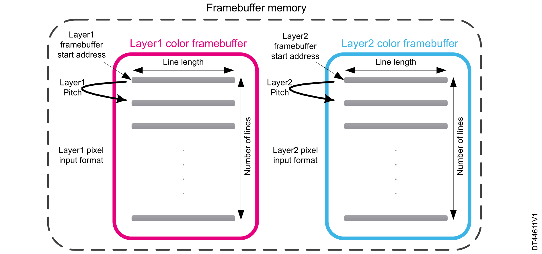
Every layer has a dedicated configurable number of lines and line length for the color framebuffer and for the pitch.

Color framebuffer address

Every layer has a start address for the color framebuffer configured through the LTDC_LxCFBAR register.

Color framebuffer length (size)

The line length and the number of lines parameters are used to stop the prefetching of data to the FIFO layer at the end of the framebuffer.

The line length (in bytes) is configurable in the LTDC_LxCFBLR register.

The number of lines (in bytes) is configurable in the LTDC_LxCFBLNR register.

Color framebuffer pitch

The pitch is the distance between the start of one line and the beginning of the next line in bytes. It is configured in the LTDC_LxCFBLR register.

Pixel input format

The programmable pixel format is used in all the data stored in the framebuffer of each LTDC layer.

For each layer, a specific pixel input format can be configured separately. The LTDC can be configured with up to eight programmable input color formats per layer.

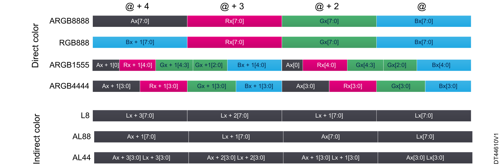
Figure 19 Pixel data mapping versus color format illustrates the pixel data mapping versus the selected input color format.

Figure 19. Pixel data mapping versus color format


Figure 20 Programmable color layer in framebuffer summarizes all layer color framebuffer configurable parameters.

Figure 20. Programmable color layer in framebuffer


Pixel format conversion (PFC)

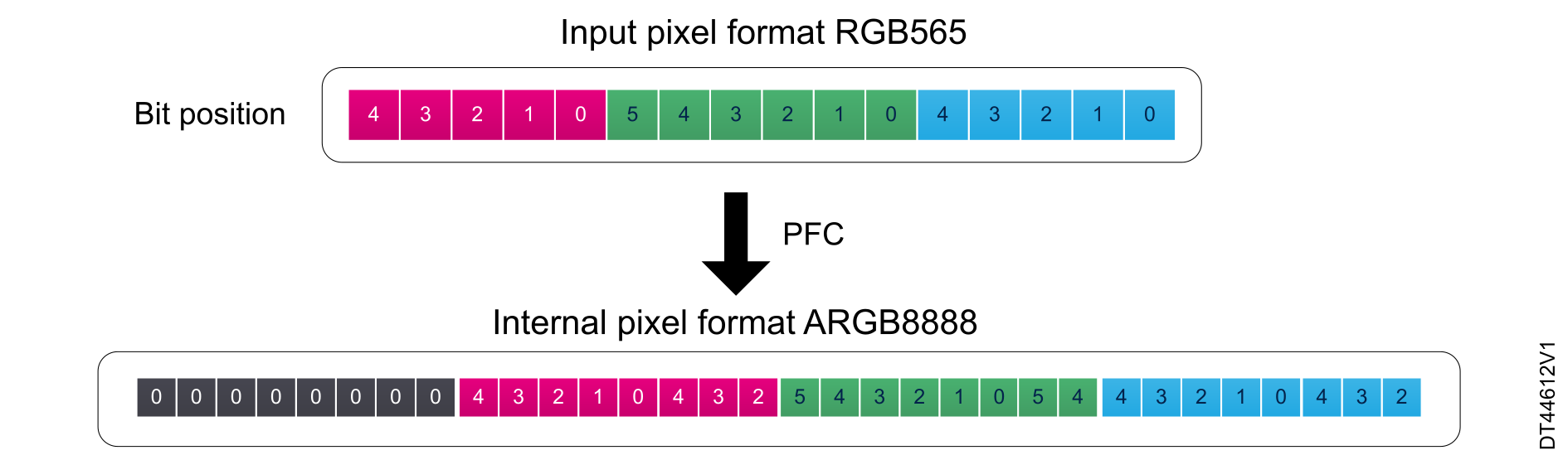
After being read from the framebuffer, the pixel data is transformed from the configured pixel input format to the internal ARGB8888 format.

The components that have a width of less than 8 bits, get expanded to 8 bits by bit replication. The MSB bits are chosen.

Figure 21 Pixel format conversion from RGB565 input pixel format to the internal ARGB8888 format shows a conversion from RGB565 input pixel format to the internal ARGB8888 format.

Figure 21. Pixel format conversion from RGB565 input pixel format to the internal ARGB8888 format


Note:

Using two layers creates bandwidth constraints on the system. It is preferable to use only one layer and to do the composition with the Chrom-Art Accelerator during the framebuffer calculation (see Checking display compatibility considering the memory bandwidth requirements).

Interrupts

The LTDC peripheral supports two global interrupts:

  • LTDC global interrupt
  • LTDC global error interrupt

Each global interrupt is connected to two LTDC interrupts (logically disjointed) that can be masked separately through a specific register. Table 7 LTDC interrupts summary summarizes all of the related interrupts and all the particular cases when each interrupt is generated.

Table 7. LTDC interrupts summary
Related NVIC interruptInterrupt eventEvent flag bit (LTDC_ISR register)Enable bit (LTDC_IER register)Clear bit (LTDC_ICR register)Description
LTDC GLOBAL INTERRUPTLineLIFLIECLIFGenerated when a defined line on the screen is reached
Register reloadRRIFRRIE CRRIFGenerated when the shadow reload occurs
LTDC GLOBAL ERROR INTERRUPTFIFO underrun1FUIFFUIE CFUIFGenerated when a pixel is requested while the FIFO is empty
Transfer errorTERRIF TERRIECTERRIFGenerated when bus error occurs
1 FIFO underrun interrupt is useful for determining the display size compatibility (see Checking display compatibility considering the memory bandwidth requirements).

Low-power modes

The STM32 power state has a direct effect on the LTDC peripheral. While in Sleep mode, the LTDC is not affected and keeps driving graphical data to the screen. While in Standby and Stop modes, the LTDC is disabled and no output is driven through its parallel interface. Exiting Standby mode must be followed with the LTDC reconfiguration.

A display panel can be driven in Sleep mode while the CPU is stopped, thanks to the smart architecture embedded in the STM32 MCUs that allows all peripherals to be enabled even in Sleep mode. This feature fits wearable applications where the low-power consumption is a must.

The LTDC, as an AHB/AXI master, can continue fetching data from FMC_SDRAM, Quad-SPI or Octo-SPI (when the Memory-mapped mode is used), even after the CPU enters Sleep mode. A line event or register reload interrupt can be generated to wake up the STM32 when a defined line on the screen is reached or when the shadow reload occurs.

More information on reducing power consumption is available on Saving power consumption.

Table 8 LTDC peripheral state versus STM32 low-power modes summarizes the LTDC state versus the STM32 low-power modes.

Table 8. LTDC peripheral state versus STM32 low-power modes
ModeDescription
RunActive
Sleep

Active
Peripheral interrupts cause the device to exit Sleep mode.

Stop

Frozen
Peripheral registers content is kept.

Standby

Powered-down
The peripheral must be reinitialized after exiting Standby mode.