AN4861 · Application noteIntroduction to LCD-TFT display controller (LTDC) on STM32 MCUs
Download .pdfOpen in the full document

Special recommendations for Cortex M7 (STM32F7/H7) and Cortex M55 (STM32N6)

Special recommendations for Cortex M7 (STM32F7/H7) and Cortex M55 (STM32N6)

This section illustrates some recommendations for the STM32F7/H7 devices embedding the Cortex-M7 CPU and for the STM32N6 devices embedding the Cortex-M55 CPU.

These recommendations are specific to the Cortex M7 and Cortex M55 since they have the following particularities compared to the Cortex M4 and Cortex M33:

  • Cortex-M7 and Cortex-M55 CPUs perform some speculative read accesses to normal memory regions.
    These speculative read accesses may cause high latency or system errors when performed on external memories over FMC, Quad-SPI, Octo-SPI, or XSPI. This impacts AHB/AXI masters (such as LTDC) accessing these external memories, and particularly decreases graphical performances and may lead to system errors (if the LTDC framebuffer is located in external memory and/or if the Quad-SPI memory is used for graphics).

  • Cortex-M7 and Cortex-M55 CPUs embed an L1-Cache.
    Some graphic issues may be encountered due to unsuitable cache settings. Bad graphic visual effects may occur if cache maintenance is not properly performed. If the suitable cache maintenance method is not used, graphical performances may be impacted.

Disable FMC Bank1 if not used

After reset, the FMC Bank1 is always enabled to allow boot into external memories. Since Cortex-M7 and Cortex-M55 perform some speculations, it can generate a speculative read access to the first FMC bank.

The default FMC configuration being very slow, this speculative access blocks the access to the FMC by other masters for a very long time, leading to underrun on the LTDC side.

To prevent CPU speculative read accesses on FMC Bank1, it is recommended to disable it when it is not used. This can be done by resetting the MBKEN Bit in FMC_BCR1 register that is, by default, enabled after reset.

To disable the FMC Bank1, the following code can be used in STM32F7 series:

/* Disabling FMC Bank1: After reset FMC_BCR1 = 0x000030DB where MBKEN = 1b meaning that FMC_Bank1 is enabled
and MTYP[1:0]= 10 meaning that memory type is set to NOR Flash/OneNAND Flash*/
FMC_Bank1->BTCR[0] = 0x000030D2;

For more details on FMC configuration, refer to the STM32 product reference manual.

Configure the memory protection unit (MPU)

This section defines the STM32F7/H7 system memory attributes and the basic MPU concepts. It also describes how to configure the MPU in order to prevent graphical performance issues related to the Cortex-M7 speculative read accesses and cache maintenance.

Note: This section only describes some necessary basic MPU concepts needed for configuration.

For further details on MPU and cache, refer to the documents AN4861_General-information.html#id_62127__entry_hzp_sky_31c, AN4861_General-information.html#id_62127__entry_mmt_sky_31c, AN4861_General-information.html#id_62127__entry_qfz_yky_31c, AN4861_General-information.html#id_62127__entry_vgb_5rx_31c, the Arm Cortex-M7 technical reference manual, and the Arm Cortex-M55 technical reference manual..

MPU attributes configuration

In order to prevent graphic performance issues related to the Cortex-M7/M55 speculative read accesses, the user must review all the memory map of the application and configure the MPU according to the hardware. So, the user has to set the following configurations:

  • Define the framebuffer MPU region and the other application MPU regions.
  • MPU must be configured according to the size of the memory used by the application.
  • The MPU attributes of the unused regions must be configured to device or strongly ordered (see Note) and Execute Never (XN). For example, for the Quad-SPI, if an 8-Mbyte memory is connected, the remaining 248-Mbyte unused space (from a total 256-Mbyte addressable space) must be set to device or strongly ordered (see Note) and Execute Never (XN). See example in MPU and cache configuration.
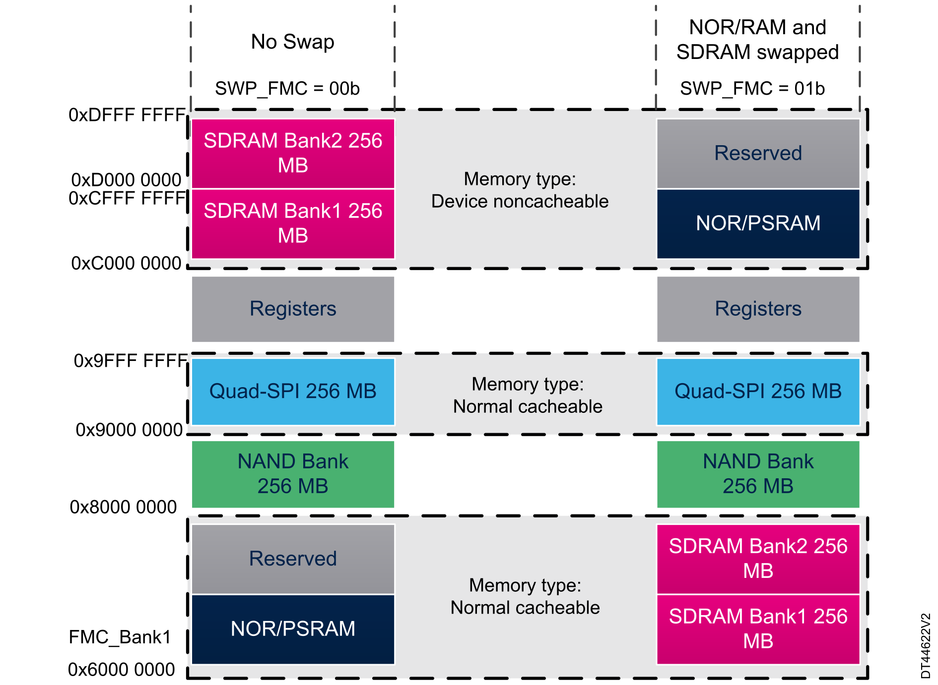
  • Prevent the Cortex-M7/M55 speculative read accesses to the external SDRAM/SRAM (if the FMC swap is enabled, see Figure 30 FMC SDRAM and NOR/PSRAM memory swap at default system memory map (MPU disabled)). To do it, the SDRAM/SRAM MPU region must be set to device or strongly ordered (see Note) and Execute Never (XN).
  • If the Cortex-M7/M55 CPU is used for framebuffer processing (writing to SDRAM/SRAM), the framebuffer region MPU attribute must be set to normal cacheable with read and write access permission.
Note:
Note:

The framebuffer MPU region attribute must be set to execute never since it is only dedicated for graphical content creation.

Figure 30 FMC SDRAM and NOR/PSRAM memory swap at default system memory map (MPU disabled) describes the STM32F7 FMC banks and Quad-SPI MPU memory attributes at default system memory map

Figure 30. FMC SDRAM and NOR/PSRAM memory swap at default system memory map (MPU disabled)


MPU and cache policy configuration

The use of Cortex-M7/M55 cache allows system and graphic performances to be boosted. This performance gain is especially seen when the CPU accesses external memories such as SDRAM or Quad-SPI.

In a graphical application, when the CPU is used for framebuffer processing, it is recommended to use the cache especially if the framebuffer is located in an external memory like SDRAM or SRAM. In that case, the user must consider the following points when using the cache:

  • MPU memory region cacheability

    As previously illustrated in Figure 30 FMC SDRAM and NOR/PSRAM memory swap at default system memory map (MPU disabled), in the default system memory region MPU attributes, some system memory regions are normal cacheable while others are device noncacheable.

    When the CPU is used for framebuffer processing, the user must change the framebuffer region MPU attribute to normal cacheable (or do an FMC swap, see Figure 30 FMC SDRAM and NOR/PSRAM memory swap at default system memory map (MPU disabled)).

  • Cache maintenance and data coherency: visual impact of WBWA without cache maintenance operation
  • The data coherency issue is often encountered when performing framebuffer processing using a Cortex‑M7/M55 CPU with L1-cache enabled and a WBWA cache policy. This issue occurs when multiple masters such as Cortex‑M7/M55 and LTDC share the same region (framebuffer) and the cache maintenance is not performed.

    When the CPU processes the framebuffer (writes to framebuffer), and if the framebuffer region has a write-back cache policy, the processed result (image to be displayed) is not seen on the framebuffer (may be SRAM or SDRAM), and then it is not displayed.

    To avoid this issue, the following methods can be used:

    • Configure the framebuffer region cache attribute to write-through (WT). In that case, each write operation is performed on the cache and on the framebuffer.
      Note:

      For some products, there is a limitation with the write-through policy. Use the write-back policy as stated in the second method. For more details about this limitation, refer to the product related errata sheet.

    • Configure the framebuffer region cache attribute to write back write allocate (WBWA) and perform the cache maintenance by software.

    Write-through is safer for data coherency but may impact graphic performances.

  • Cache maintenance may impact graphic performances

    The suitable cache policy matching the application must be used. Each method has its cons and pros, so the user must consider the following particularities for each method:

    • Write-through is very simple to manage (no need to perform cache maintenance by software) and safer for data coherency but it generates a lot of single-write operations to the framebuffer, which may impact LTDC accesses.
      Note:

      The user must also consider that cache maintenance may impact graphic performances even when the CPU is not used for framebuffer processing. Thus, in some applications, the CPU accesses the external SDRAM or SRAM for other purposes than graphics with cache enabled. In that case, cache maintenance may impact the LTDC accesses.

    • Write-back-write allocate: it is more suitable to use WBWA and software routine and to synchronize the cache maintenance operation with the LTDC during blanking. This allows an additional bandwidth creation on the framebuffer memory (SRAM or SDRAM). The cache maintenance operation need to be performed by software after writing data to the framebuffer memory region. This is done by forcing a D-cache clean operation using the CMSIS function SCB_CleanDCache(). So, all the dirty lines in the cache are written back to the framebuffer.

MPU configuration example

An example of MPU configuration is described in MPU and cache configuration, showing how to set the framebuffer MPU attribute when the CPU is used (with cache enabled) for graphical operations. The described example is created for the STM32F746G-DISCO board hardware configuration, where the external SDRAM is used for framebuffer and the external Quad-SPI flash memory contains the graphic primitives.

LTDC peripheral configuration

This section describes the steps needed to configure the LTDC peripheral.

Note:

It is recommended to reset the LTDC peripheral before starting the configuration and it is also recommended to guarantee that the peripheral is in reset state. The LTDC can be reset by setting the corresponding bit in the RCC_APB2RSTR register, which resets the three clock domains.

Display panel connection

The LTDC hardware interface provides eight bits per color bus, and fits perfectly for RGB888 true color panels. The LTDC hardware interface provides also timing signals: LCD_HSYNC, LCD_VSYNC, LCD_DE, and LCD_CLK.

The LTDC GPIOs must be configured to the correspondent alternate function. For more details on LTDC alternate functions availability versus GPIOs, refer to the alternate function mapping table in the product datasheet.

Note:

All GPIOs have to be configured in very-high-speed mode.

Connecting lower palette display panels

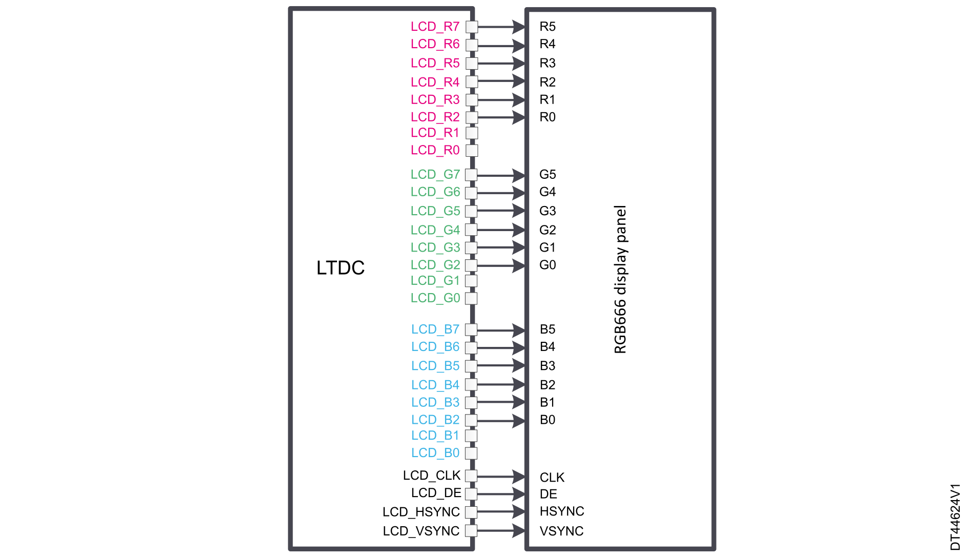
For display panels with a lower color palette (such as RGB666 and RGB565), the bus connection must be done with the most significant bits of the data signals. Figure 31 Connecting an RGB666 display panel shows an example of connecting an RGB666 display panel.

Figure 31. Connecting an RGB666 display panel


GPIOs configuration using STM32CubeMX tool

To connect a display panel to an STM32 MCU, the user must configure the GPIOs to be used for interfacing.

Using the STM32CubeMX tool is a very simple, easy, and rapid way to configure the LTDC peripheral and its GPIOs, since it allows a project to be generated with a preconfigured LTDC (see LTDC GPIOs configuration).

Configuration of specific pins of a display module

Some display modules may need other signals to be fully functional. GPIOs and some peripherals can be used to control these signals.

An example of using GPIOs to control the displayenable pin (LCD_DISP) on a display panel is described in LTDC GPIOs configuration.

Enabling LTDC interrupts

To be able to use the LTDC interrupts, the user must enable the LTDC global interrupts on the NVIC side. Then, each interrupt is enabled separately by enabling its corresponding enable bit. The LTDC interrupt-enable bits are available in the LTDC_IER register described in Table 7 LTDC interrupts summary.

Note:

The FIFO underrun and transfer error interrupts are enabled in the hal_ltdc driver HAL_LTDC_Init() function

An example of enabling LTDC interrupts using STM32CubeMX is described in LTDC GPIOs configuration

LTDC clocks and timings configuration

This section describes the steps needed to configure the LTDC clock and timings respecting the display specifications. It also provides a configuration example for the ROCKTECH (RK043FN48H) display embedded on the STM32F746G-DISCO board.

System clock configuration

It is recommended to use the highest system clock to get the best graphic performances. This recommendation applies also for the external memory framebuffer. So, if an external memory is used for the framebuffer, the highest allowed clock speed must be used to get the best memory bandwidth.

For instance, for the STM32F4x9, the maximum system speed is 180 MHz. So, if an external SDRAM is connected to the FMC, the maximum SDRAM clock is 90 MHz (HCLK/2).

For the STM32F7, the maximum system speed is 216 MHz but with this speed and HCLK/2 prescaler the SDRAM speed exceeds the maximum allowed speed (see product datasheet for more details). So, to get the maximum SDRAM, it is recommended to configure HCLK to 200 MHz, then the SDRAM speed is set to 100 MHz.

The clock configuration providing the highest performances is:

  • STM32F4x9:HCLK @ 180 MHz and SDRAM @ 90 MHz
  • STM32F7:HCLK @ 200 MHz and SDRAM @ 100 MHz

An example of LTDC configuration using STM32CubeMX is described in LTDC peripheral configuration.

Pixel clock and timings configuration

At this stage of the graphical application development, the user must have already checked and confirmed that the desired display size and color depth are compatible with the hardware configuration. Therefore, the pixel clock to be configured must be already known, either extracted from the display datasheet or calculated (see Checking display compatibility considering the memory bandwidth requirements).

Example: LTDC timings configuration for ROCKTECH RK043FN48H display embedded on the STM32F746G-DISCO board. At first, the user must extract the timing parameters from the display datasheet (see Table 22 LCD-TFT timings extracted from ROCKTECH RK043FN48H datasheet). It is recommended to use typical display timings.

Table 22. LCD-TFT timings extracted from ROCKTECH RK043FN48H datasheet The cells in bold highlight the values used in the example presented below.
ItemSymbolMin.Typ.Max.Unit
DCLK frequencyFclk5912MHz
DCLK periodTclk83110200ns
HsyncPeriod timeTh490531605DCLK
Display periodThdisp-480-DCLK
Back porchThbp843-DCLK
Front porchThfp28-DCLK
Pulse widthThw1--DCLK
VsyncPeriod timeTv275288335H
Display periodTvdisp-272-H
Back porchTvbp212-H
Front porchTvfp14-H
Pulse widthTvw110-H

Based on the above table, the extracted timing parameters are:

  • Display period (active width) = 480 pixels
  • Back porch HBP = 43 pixels
  • Front porch HFP = 8 pixels
  • Pulse width HSYNC = 1 pixel (minimum value)
  • Display period (active height) = 272 lines
  • Vertical back porch VBP = 12 lines
  • Front porch VFP = 4 lines
  • Pulse width VSYNC = 10 lines

Program timing parameters: once timing parameters are extracted, they are used to program the LTDC timing registers, Table 23 Programming LTDC timing registers summarizes all the parameters to be programmed.

Timing parameters configuration with STM32CubeMX: it is very easy to program the timing parameters using STM32CubeMX. The user must simply fill the extracted parameters in the LTDC configuration window (see section LTDC peripheral configuration).

Table 23. Programming LTDC timing registers
Register-Value to be programmed
LTDC_SSCRHSW[11:0]HSYNC Width - 10
VSH[11:0]VSYNC Height - 19
LTDC_BPCRAHBP[11:0]HSYNC Width + HBP - 143
AVBP[10:0]VSYNC Height + VBP - 121
LTDC_AWCRAAW[11:0]HSYNC Width + HBP + Active Width - 1523
AAH[10:0]VSYNC Height + BVBP + Active Height - 1293
LTDC_TWCRTOTALW[11:0]HSYNC Width + HBP + Active Width + HFP - 1531
TOTALH[10:0]VSYNC Height+ BVBP + Active Height + VFP - 1297

Pixel clock configuration with STM32CubeMX: the pixel clock is calculated with a 60 Hz refresh rate as shown below:

LCD_CLK = TOTALW x TOTALH x refresh rate

Based on Table 23 Programming LTDC timing registers, TOTALW= 531 and TOTALH = 297.

And for this example:

LCD_CLK = 531 x 297 x 60 = 9.5 MHz

Refer to the LTDC pixel clock configuration STM32CubeMX example in LTDC peripheral configuration.

LTDC control signals polarity configuration

The LTDC control signals (HSYNC, VSYNC, DE, and LCD_CLK) polarities must be configured respecting the display specifications.

Note:

Only the DE control signal must be inverted versus the DE polarity indicated in the display datasheet. The other control signals must be configured exactly like the display datasheet.
LTDC layers configuration

This section describes the needed steps to configure the LTDC layers, respecting the display size and the color depth.

As previously stated in Programmable layer: color framebuffer, the LTDC features two independently configurable layers (the user can enable either one or the two layers). By default, both layers are disabled, so only the configured background color is displayed (the default color is black).

The user can display Layer1 + background or display Layer1 + Layer2 + background.

Display only the background

If no layer are enabled, only the background is displayed. If the background color is not configured, the default background black color is displayed (LTDC_BCCR = 0x00000000).

To set a blue background color, the LTDC_BCCR register must be set to 0x000000FF.

Layer parameters configuration

Once LTDC GPIOs, clocks and timings are properly set, the user must configure the following LTDC layer parameters. Each LTDC layer has its own parameters that must be configured separately:

  • window size and position
  • pixel input format
  • framebuffer start address
  • framebuffer size (image width and image height) and pitch
  • layer default color in ARGB8888 format
  • layer constant alpha for blending
  • layer blending factor1 and factor2

An example of LTDC layer parameters configuration using STM32CubeMX is described in LTDC Layer parameters configuration.

Note:

All layer parameters can be modified on the fly, except for the CLUT. The new configuration has to be either reloaded immediately or during vertical blanking period by configuring the LTDC_SRCR register.

Display panel configuration

Some displays require to be configured using serial communication interfaces such as I2C or SPI.

For instance, the STM32F429I-DISCO embeds the ILI9341 display module that is initialized through the SPI interface.

A dedicated driver for this display module (ili9341.c), including initialization and configuration commands, is available in the STM32Cube firmware package under:STM32Cube_FW_F4_Vx.xx.x\Drivers\BSP\Components\ili9341

An example of display initialization sequence based on the ili9341_Init() function is included in the STM32Cube examples for the STM32F429I-Discovery board under:STM32Cube_FW_F4_Vx.xx.x\Projects\STM32F429I-Discovery\Examples\LTDC\LTDC_Display_2Layers