製品概要
主な利点
65W高効率設計
ZVS準共振フライバックにより、最大65Wの出力を実現し、小型で発熱の少ないアダプタを実現
コンパクトで高集積なソリューション
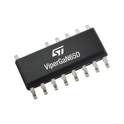
SO16Nパッケージに収められた700V GaNトランジスタを搭載した高度なPWMコントローラ
堅牢な保護機能を内蔵
OVP、OCP、ブラウンイン/ブラウンアウト、iOVP、OTP機能を搭載し、安全で長寿命な動作を保証
概要
The VIPERGAN65D is a high voltage converter, designed for medium power quasi-resonant ZVS (Zero Voltage Switching at switch turn-on) flyback converters, capable to provide an output power up to 65 W in wide range.

It integrates a complete set of features that provide an extremely flexible and easy to use chip and helps to design a highly efficient offline power supply. The ZVS quasi-resonant operation with the dynamic blanking time feature and the valley synchronization function, that turns on the power switch always at the valley of the drain resonance, reduces the switching losses and maximizes the overall efficiency at any input line and load condition. The advanced power management with the low quiescent helps to achieve low stand-by consumptions. The feed-forward compensation minimizes the maximum output peak power variation over the entire input voltage range.
In addition to the above functions, the device offers protection features that considerably increase end-product’s safety and reliability: the output overvoltage protection (OVP), the overload protection (OLP), the brown-in/out protection, that set the input voltage level to power on and power off the converter and the input overvoltage protection (iOVP), that protects the system in case of an abnormal increase of the input line. All the protections are auto-restart mode.
-
機能一覧
- Quasi-resonant (QR) flyback controller
- 700 V E-mode power GaN transistor
- Embedded sense FET
- Dynamic blanking time and adjustable valley synchronization delay functions, to maximize efficiency at any input line and load condition
- Valley-lock to ensure constant valley skipping
- Advanced power management for less than 30 mW standby power consumption with adaptive burst-mode
- Output overvoltage protection (OVP)
- Input voltage feed-forward compensation for mains independent OPP variation
- Brown-in and brown-out protection
- Input overvoltage protection (iOVP)
- Output overload protection (OVL)
- Output rectifier short circuit protection (OCP_LEB)
- Embedded thermal shutdown
- Frequency jitter for EMI suppression
eDesignSuite
eDesignSuiteは、幅広いST製品を用いたシステム開発プロセスの効率化を支援する、使いやすい設計支援ユーティリティの包括的なセットです。

パワー・マネージメント設計センター
デバイス用熱電気シミュレータ
シグナル・コンディショニング設計ツール
NFC / RFIDカリキュレータ
パワー・マネージメント設計センター

電源設計ツール
パワー・マネージメント設計センター

LED照明設計ツール
パワー・マネージメント設計センター

デジタル電源ワークベンチ
パワー・マネージメント設計センター

パワー・ツリー・デザイナ
デバイス用熱電気シミュレータ

STPOWER Studio
デバイス用熱電気シミュレータ

PCB Thermal Simulator
デバイス用熱電気シミュレータ

ACスイッチ・シミュレータ
デバイス用熱電気シミュレータ

整流ダイオード・シミュレータ
デバイス用熱電気シミュレータ

TwisterSim
デバイス用熱電気シミュレータ

TVSシミュレータ
デバイス用熱電気シミュレータ

Estimate
シグナル・コンディショニング設計ツール

アクティブ・フィルタ
シグナル・コンディショニング設計ツール

コンパレータ(ウィンドウ・コンパレータ機能搭載)
シグナル・コンディショニング設計ツール

ローサイド電流センス・アンプ
シグナル・コンディショニング設計ツール

ハイサイド電流センス・アンプ
NFC / RFIDカリキュレータ

NFCインダクタンス
NFC / RFIDカリキュレータ

UHFリンク・バジェット
NFC / RFIDカリキュレータ

NFCチューニング回路
Featured Videos

EDA Symbols, Footprints and 3D Models
STMicroelectronics - VIPERGAN65D
Speed up your design by downloading all the EDA symbols, footprints and 3D models for your application. You have access to a large number of CAD formats to fit with your design toolchain.
Please select one model supplier :

Symbols

Footprints

3D models
すべてのリソース
| Resource title | Version | Latest update | Actions | Details | ダウンロード |
|---|
SIMPLIS models (1)
| Resource title | Version | Latest update | Actions | Options | ||
|---|---|---|---|---|---|---|
| ZIP | 12.2024 | 10 Jul 2025 | 10 Jul 2025 |
Quality and Reliability
| Part Number | Marketing Status | Package | Grade | RoHSコンプライアンスグレード | Longevity Commitment | Longevity Starting Date | Material Declaration** |
|---|---|---|---|---|---|---|---|
| VIPERGAN65DTR | Active 交換品交換品 | SOIC 14 DEPOPULATED PINS | Industrial | Ecopack2 | - | - |
(**) st.comで提供している材料宣誓書は、パッケージ・ファミリ内で最も一般的に使用されているパッケージに基づく汎用ドキュメントの場合があります。そのため、特定の製品では100%正確ではない可能性があります。特定の製品情報については、セールスサポートまでお問い合わせください

You’re now leaving st.com and will be re-directed to our Partner’s website.
For the latest innovations and solutions from ST, sign up for our newsletters.
Sample & Buy

| Part Number | 製品ステータス | Budgetary Price (US$)*/Qty | STから購入 | Order from distributors | Package | Packing Type | RoHS | Country of Origin | ECCN (US) | ECCN (EU) | Operating temperature (°C) | Operating Temperature (°C) (max) | Transistor Breakdown Voltage (V) (min) | Drain Current (A) (nom) | RDS(on) (Ω) (max) | ||
|---|---|---|---|---|---|---|---|---|---|---|---|---|---|---|---|---|---|
| 最小 | 最大 | ||||||||||||||||
| VIPERGAN65DTR | | | distributors 販売代理店に在庫がない場合は、STのセールス・オフィスまでお問い合わせください |
|
|
| |||||||||||
VIPERGAN65DTR Active
販売代理店に在庫がない場合は、STのセールス・オフィスまでお問い合わせください
(*)概算用の参考価格(US$)です。現地通貨でのお見積りについては、STのセールス・オフィスまたは販売代理店までお問い合わせください。