![]() STのパワーMOSFET製品ポートフォリオは、-100V~1700Vという広範囲のブレークダウン電圧を提供するだけでなく、最先端のパッケージに低いゲート電荷とオン抵抗を兼ね備えています。STのプロセス技術では、MDmeshおよびSTMESHトレンチ高電圧パワーMOSFETとSTripFET低電圧パワーMOSFETで電力処理を強化することにより、高効率のソリューションを実現します。
STのパワーMOSFET製品ポートフォリオは、-100V~1700Vという広範囲のブレークダウン電圧を提供するだけでなく、最先端のパッケージに低いゲート電荷とオン抵抗を兼ね備えています。STのプロセス技術では、MDmeshおよびSTMESHトレンチ高電圧パワーMOSFETとSTripFET低電圧パワーMOSFETで電力処理を強化することにより、高効率のソリューションを実現します。
アプリケーション


製品タイプ
STは、スイッチモード電源(SMPS)、照明、モータ制御、エネルギー生成とeモビリティ、シャーシ & セーフティ、さらにボディ & コンビニエンスといった産業および車載用アプリケーションのあらゆる電圧範囲に対応できるパワーMOSFETを幅広く扱っています。
製品ポートフォリオの詳細はこちら

メリット
- -100V~1700Vの耐圧範囲
- 低電圧~超高耐圧のパワーMOSFETに対応できる以下を含む30以上のパッケージ・オプションをご用意しています。
- さらに高い電力密度で温度管理も改善する新しい上面冷却型HU3PAKパッケージ
- スイッチング効率を向上させる専用制御ピンを備えた4ピンTO-247
- 大電流容量のH2PAK
- 革新的な表面実装型リードレスTO-LL
- 大型の金属ドレイン・パッドを採用することで優れた熱性能を実現した高さ1mmの表面実装型PowerFLATファミリ(2mm x 2mm~8mm x 8mm)
- 最先端の厳しい効率要件に応じて改良されたゲート電荷量およびオン抵抗
- 厳選された製品ライン向けの高速ボディ・ダイオード内蔵オプション
- 車載グレード対応パワーMOSFETの幅広い製品ポートフォリオ
- アプリケーション指向テクノロジー
Featured Videos

 MOSFET: Technologies and nomenclature")

推奨コンテンツ
Automotive MOSFETs in tiny 5x6 mm dual-side cooling package
Power MOSFET Basics
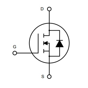
MOSFET stands for Metal Oxide Semiconductor Field Effect Transistor. It's a voltage controlled device with 3 terminals:
- Gate (electrically insulated from the semiconductor)
- Drain
- Source
When a voltage applied between the Gate and the Source reaches a certain threshold (VGS(th) or threshold G-S voltage), the device is able to support current conduction between the Drain and the Source (ID or drain current).
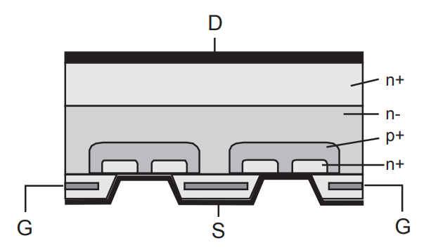
When a voltage applied between the Gate and the Source is below VGS(th), the device will withstand a voltage up to BVDSS (or breakdown voltage).
MOSFETs can be used as a signal amplifier (linear operation) or as a switch in power applications.
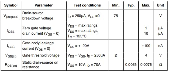
MOSFET parameters
Like many other types of semiconductor power switches, the main parameters of a MOSFET, usually available in most datasheets, are:
- RDS(on) (on-state resistance): electrical resistance when the device is set in on state. The lower is RDS(on), the lower is the conduction loss due to power dissipation when the current is flowing.
- BVDSS (breakdown voltage): maximum drain-to-source voltage that the device is able to sustain when in off state.
- QG (total gate charge): amount of electric charge required to the gate driver to turn on/off the device itself. QG impacts directly the efficiency (the lower, the better).
The product of RDS(on) and QG is known as the MOSFET Figure of Merit (FOM).
Other important parameters are intrinsic capacitances that can affect the switching times and voltage spikes, and body drain diode when device is used as power diode, like in synchronous free-wheeling operation mode.
Learn more about how to read MOSFET datasheet parameters thanks to our series of videos dedicated to "Power MOSFET datasheet parameters".
Main types of power MOSFETs
MOSFETs can be of different types, including:
- Depletion Mode: Normally ON. Applying the VGS would turn it OFF.
- Enhancement Mode: Normally OFF. Applying the VGS would turn it ON.
- N-channel MOSFETs: positive voltages and currents.
- P-channel MOSFETs: negative voltages and currents.
- Low voltage MOSFETs: BVDSS from 0 V to 200 V.
- High voltage MOSFETs: BVDSS greather than 200 V.
N-channel enhancement-mode MOSFETs are the most popular type used in power switching circuits because of their low RDS(on) (on-state resistance) compared to P-channel MOSFETs.

Power MOSFET Applications
Power MOSFETs play an important role in all applications handling Power.
The main applications of high voltage MOSFETs include:
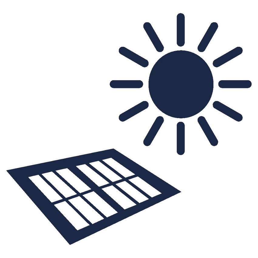
- Switch Mode Power Supplies (SMPS)
- Residential, commercial, architectural and street lighting
- DC-DC converters
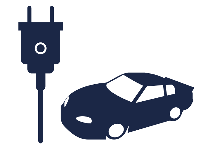
- Motor control
- Automotive applications
ST's high voltage MOSFET portfolio offers a broad range of breakdown voltages up to 1700 V, with low gate charge and low on-resistance, combined with state-of-the-art packaging. ST's MDmesh™ high-voltage MOSFETs technology has enhanced power-handling capability, resulting in high-efficiency solutions.
The main applications of low voltage MOSFETs include:
- Switch, buck and synchronous rectification
- Uninterruptible Power Supplies (UPS)
- Small motor control
- Switch Mode Power Supplies (SMPS)
- Power-Over-Ethernet (PoE)
- Solar inverters
- Automotive applications
ST's low voltage MOSFET portfolio offers a broad range of breakdown voltages from -100 V to 120 V, with low gate charge and low on-resistance, combined with state-of-the art packaging.
eDesignSuite
eDesignSuiteは、幅広いST製品を用いたシステム開発プロセスの効率化を支援する、使いやすい設計支援ユーティリティの包括的なセットです。

パワー・マネージメント設計センター
デバイス用熱電気シミュレータ
シグナル・コンディショニング設計ツール
NFC / RFIDカリキュレータ
パワー・マネージメント設計センター

電源設計ツール
パワー・マネージメント設計センター

LED照明設計ツール
パワー・マネージメント設計センター

デジタル電源ワークベンチ
パワー・マネージメント設計センター

パワー・ツリー・デザイナ
デバイス用熱電気シミュレータ

STPOWER Studio
デバイス用熱電気シミュレータ

PCB Thermal Simulator
デバイス用熱電気シミュレータ

ACスイッチ・シミュレータ
デバイス用熱電気シミュレータ

整流ダイオード・シミュレータ
デバイス用熱電気シミュレータ

TwisterSim
デバイス用熱電気シミュレータ

TVSシミュレータ
デバイス用熱電気シミュレータ
Estimate
シグナル・コンディショニング設計ツール

アクティブ・フィルタ
シグナル・コンディショニング設計ツール

コンパレータ(ウィンドウ・コンパレータ機能搭載)
シグナル・コンディショニング設計ツール

ローサイド電流センス・アンプ
シグナル・コンディショニング設計ツール

ハイサイド電流センス・アンプ
NFC / RFIDカリキュレータ

NFCインダクタンス
NFC / RFIDカリキュレータ

UHFリンク・バジェット
NFC / RFIDカリキュレータ
