The ST power MOSFET portfolio offers a broad range of breakdown voltages from -100 to 1700 V, combining state-of-the-art packaging with low gate charge and low on-resistance. Our process technology ensures high-efficiency solutions through enhanced power handling with MDmesh and STMESH trench high-voltage power MOSFETs and STripFET low-voltage power MOSFETs.
Product types
ST offers an impressive range of Power MOSFETs for any voltage range in industrial and automotive applications, such as switch mode power supplies (SMPS), lighting, motor control, energy generation & electro mobility, chassis & safety, and body & convenience.
Discover our portfolio

Benefits
- -100 to 1700 V breakdown voltage range
- More than 30 package options for low voltage to very-high-voltage Power MOSFETs, including:
- Breakthrough top-side cooling HU3PAK package allowing higher power density and improved thermal management
- 4-lead TO-247 with dedicated control pin for increased switching efficiency
- H2PAK for high-current capability
- Highly innovative surface-mount leadless TO-LL
- 1-mm-high surface-mount PowerFLAT family (2x2 to 8x8 mm) with excellent thermal performance thanks to large metal drain pad
- Improved gate charge and lower on-state resistance to meet today's challenging efficiency requirements
- Intrinsic fast body diode option for selected product lines
- Wide portfolio of automotive-grade power MOSFETs
- Application-oriented technologies
Featured Videos
Recommended for you
Automotive MOSFETs in tiny 5x6 mm dual-side cooling package
ST has extended its offering of AEC-Q101 MOSFETs with the introduction of two 40 V devices in the advanced PowerFLAT™ 5x6 dual-side cooling (DSC) package with wettable flanks. The STLD200N4F6AG and STLD125N4F6AG, with a maximum on-resistance of 1.5 mΩ and 3.0 mΩ respectively, ensure high efficiency and help simplify system thermal management. The 0.8 mm-high PowerFLAT 5x6 DSC retains the footprint and thermally efficient bottom-side design of the standard wettable flank package, while it exposes the top-side source electrode to further enhance heat dissipation. This allows a higher current rating that increases power density, enabling designers to build smaller ECUs without trading off functionality, performance, or reliability.
Power MOSFET Basics

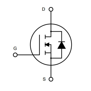
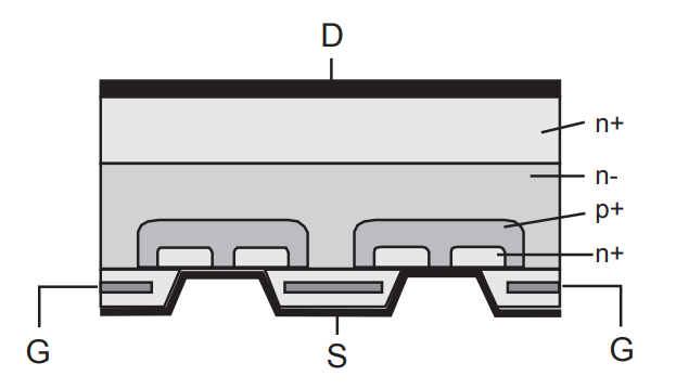
MOSFET stands for Metal Oxide Semiconductor Field Effect Transistor. It's a voltage controlled device with 3 terminals:
- Gate (electrically insulated from the semiconductor)
- Drain
- Source
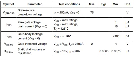
When a voltage applied between the Gate and the Source reaches a certain threshold (VGS(th) or threshold G-S voltage), the device is able to support current conduction between the Drain and the Source (ID or drain current).

When a voltage applied between the Gate and the Source is below VGS(th), the device will withstand a voltage up to BVDSS (or breakdown voltage).
MOSFETs can be used as a signal amplifier (linear operation) or as a switch in power applications.
MOSFET parameters
Like many other types of semiconductor power switches, the main parameters of a MOSFET, usually available in most datasheets, are:
- RDS(on) (on-state resistance): electrical resistance when the device is set in on state. The lower is RDS(on), the lower is the conduction loss due to power dissipation when the current is flowing.
- BVDSS (breakdown voltage): maximum drain-to-source voltage that the device is able to sustain when in off state.
- QG (total gate charge): amount of electric charge required to the gate driver to turn on/off the device itself. QG impacts directly the efficiency (the lower, the better).
The product of RDS(on) and QG is known as the MOSFET Figure of Merit (FOM).
Other important parameters are intrinsic capacitances that can affect the switching times and voltage spikes, and body drain diode when device is used as power diode, like in synchronous free-wheeling operation mode.

Learn more about how to read MOSFET datasheet parameters thanks to our series of videos dedicated to "Power MOSFET datasheet parameters".
Main types of power MOSFETs
MOSFETs can be of different types, including:
- Depletion Mode: Normally ON. Applying the VGS would turn it OFF.
- Enhancement Mode: Normally OFF. Applying the VGS would turn it ON.
- N-channel MOSFETs: positive voltages and currents.
- P-channel MOSFETs: negative voltages and currents.
- Low voltage MOSFETs: BVDSS from 0 V to 200 V.
- High voltage MOSFETs: BVDSS greather than 200 V.
N-channel enhancement-mode MOSFETs are the most popular type used in power switching circuits because of their low RDS(on) (on-state resistance) compared to P-channel MOSFETs.

Power MOSFET Applications
Power MOSFETs play an important role in all applications handling Power.
The main applications of high voltage MOSFETs include:
- Switch Mode Power Supplies (SMPS)
- Residential, commercial, architectural and street lighting
- DC-DC converters
- Motor control
- Automotive applications
ST's high voltage MOSFET portfolio offers a broad range of breakdown voltages up to 1700 V, with low gate charge and low on-resistance, combined with state-of-the-art packaging. ST's MDmesh™ high-voltage MOSFETs technology has enhanced power-handling capability, resulting in high-efficiency solutions.
The main applications of low voltage MOSFETs include:
- Switch, buck and synchronous rectification
- Uninterruptible Power Supplies (UPS)
- Small motor control
- Switch Mode Power Supplies (SMPS)
- Power-Over-Ethernet (PoE)
- Solar inverters
- Automotive applications
ST's low voltage MOSFET portfolio offers a broad range of breakdown voltages from -100 V to 120 V, with low gate charge and low on-resistance, combined with state-of-the art packaging.
eDesignSuite
eDesignSuite is a comprehensive set of easy-to-use design-aid utilities ready to help you streamline the system development process with a wide range of ST products.

Power Management Design Center
Thermal-electrical Simulators for Components Test
Signal Conditioning Design Tool
NFC/RFID Calculators
Power Management Design Center

Power Supply Design Tool Test
Power Management Design Center

LED Lighting Design Tool
Power Management Design Center

Digital Power Workbench
Power Management Design Center

Power Tree Designer
Thermal-electrical Simulators for Components Test

STPOWER Studio
Thermal-electrical Simulators for Components Test

PCB Thermal Simulator
Thermal-electrical Simulators for Components Test

AC Switches Simulator test
Thermal-electrical Simulators for Components Test

Rectifier Diodes Simulator test
Thermal-electrical Simulators for Components Test

Twister Sim
Thermal-electrical Simulators for Components Test

TVS Simulator
Thermal-electrical Simulators for Components Test

Estimate
Signal Conditioning Design Tool

Active Filters
Signal Conditioning Design Tool

Comparators
Signal Conditioning Design Tool

Low side Current Sensing
Signal Conditioning Design Tool

High side Current Sensing
NFC/RFID Calculators

NFC Inductance
NFC/RFID Calculators

UHF Link Budget
NFC/RFID Calculators


