TO-LL leadless and SMD thermally efficient package for high power applications
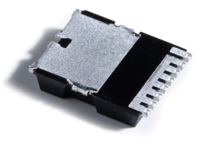
The TO-LL package offers an excellent balance between heat management, current capability, and PCB space. The lower Rthj-amb of the TO-LL package, combined with thermal vias and bottom heatsink on the host board, allows designers to occupy less PCB space and manage heat more efficiently than SMD and through-hole packages.
The additional Kelvin-source lead on the package also helps designers achieve higher efficiency through reduced turn-on/turn-off switching losses.
Another key characteristic is the 2.7 mm creepage between the drain and source pads, which ensures better isolation and protection from failures caused by voltage events that exceed the breakdown rating of the device.
ST offers MDmesh M6 (600V) and MDmesh DM6 (600-650V) superjunction MOSFETs in TO-LL packages targeting servers, telecom data centers, SMPS, and solar microinverters. The range of devices in TO-LL packages will be expanded with the inclusion of the latest MDmesh M9 and DM9 series of STPOWER MOSFETs. applications.
Key features and benefits
- Reduced space on PCB vs D2PAK with the same area inside
- Reduced thickness: 2.3 mm
- Large exposed drain pad
Application examples
- Additional Kelvin source pin
- High creepage: 2.7 mm

5G data centers

Server and telecom SMPS

Solar energy
Recommended resources

TO-LL leadless surface mounted packages for high-power performance
Product video
ST offers high-voltage MDmesh M6 & M9 STPOWER MOSFETs in a new compact, thermally efficient package: the TO-LL surface-mounted package offers high electrical and thermal efficiency, compactness and space saving in power conversion applications like SMPS, data centers and solar microinverters. Thanks to the additional Kelvin-source lead, designers can achieve better efficiency due to reduced turn-on/turn-off switching losses.
TO-LL: the latest evolution in SMD power packages
Brochure
The new STPOWER MOSFET Super-junction MDmesh* M6 and MDmesh DM6 series in the space-saving and thermally efficient TO-LL leadless package allows more compact and spacesaving power converters. Thanks to the additional Kelvin-source lead, designers can achieve better efficiency due to reduced turn-on / turn-off switching losses.


TO-LL and MDmesh M6 the latest breakthrough in high-level telecom SMPS
Conference paper
This paper presents the ST’s new SMD package TO-LL (TO-lead less) and its benefits in terms of thermal management, PCB area, switching performance and parasitic inductance on the leads. Thanks to this innovative SMD package and the latest Super Junction technology from ST, MDmesh M6 for PFC and MDmesh DM6 for LLC...
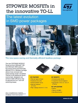
STPOWER MOSFETs in the innovative TO-LL
Flyer
The new STPOWER MOSFET Super-junction MDmesh( *) M6 and MDmesh DM6 series in the space-saving and thermally efficient TO-LL leadless package allows more compact and space-saving power converters. Thanks to the additional Kelvinsource lead, designers can achieve better efficiency due to reduced turn-on / turn-off switching losses.