Product overview
Description
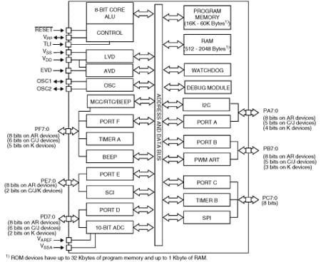
The ST72F325 Flash and ST72325 ROM devices are members of the ST7 microcontroller family designed for mid-range applications.
They are derivatives of the ST72321 and ST72324 devices, with enhanced characteristics and robust Clock Security System.
All devices are based on a common industrystandard 8-bit core, featuring an enhanced instruction set and are available with Flash or ROM program memory. The ST7 family architecture offers both power and flexibility to software developers, enabling the design of highly efficient and compact application code.
The on-chip peripherals include an A/D converter, a PWM Autoreload timer, 2 general purpose timers, I2C bus, SPI interface and an SCI interface.
For power economy, microcontroller can switch dynamically into WAIT, SLOW, ACTIVE-HALT or HALT mode when the application is in idle or stand-by state.
Typical applications are consumer, home, office and industrial products.
The devices feature an on-chip Debug Module(DM) to support in-circuit debugging (ICD). For adescription of the DM registers, refer to the ST7ICC Protocol Reference Manual.Main Differences with ST72321:
-
All features
- 1 Analog peripheral (low current coupling)
10-bit ADC with up to 16 robust input ports - 3 Communications interfaces
SPI synchronous serial interface SCI asynchronous serial interface I2C multimaster interface - Development tools
Full hardware/software development package DM (Debug module) - Memories
16K to 60K dual voltage High Density Flash (HDFlash) or up to 32K ROM with read-outprotection capability. In-Application Programming and In-Circuit Programming for HDFlash devices 512 to 2048 bytes RAM HDFlash endurance: 100 cycles, data retention: 40 years at 85°C - Interrupt management
Nested interrupt controller 14 interrupt vectors plus TRAP and RESET Top Level Interrupt (TLI) pin on 64-pin devices 9/6 external interrupt lines (on 4 vectors) - Clock, reset and supply management
Enhanced low voltage supervisor (LVD) for main supply and auxiliary voltage detector(AVD) with interrupt capability Clock sources: crystal/ceramic resonator oscillators, internal RC oscillator and bypass for external clock PLL for 2x frequency multiplication Four Power Saving Modes: Halt, Active-Halt,Wait and Slow Clock Security System - 5 timers
Main Clock Controller with: Real time base, Beep and Clock-out capabilities Configurable watchdog timer Two 16-bit timers with: 2 input captures, 2 output compares, external clock input on one timer, PWM and pulse generator modes 8-bit PWM Auto-reload timer with: 2 input captures, 4 PWM outputs, output compare and time base interrupt, external clock with event detector - Instruction set
8-bit Data Manipulation 63 Basic Instructions 17 main Addressing Modes 8 x 8 Unsigned Multiply Instruction - Up to 48 I/O ports
48/36/32/24 multifunctional bidirectional I/O lines 34/26/22/17 alternate function lines 16/13/12/10 high sink outputs
- 1 Analog peripheral (low current coupling)
Circuit Diagram
EDA Symbols, Footprints and 3D Models
STMicroelectronics - ST72325R9
Speed up your design by downloading all the EDA symbols, footprints and 3D models for your application. You have access to a large number of CAD formats to fit with your design toolchain.
Please select one model supplier :
Symbols

Footprints

3D models
All resources
| Resource title | Version | Latest update | Actions | Details | Download |
|---|
Board Manufacturing Specifications (1)
| Resource title | Version | Latest update | Actions | Options | ||
|---|---|---|---|---|---|---|
| ZIP | 1.0 | 01 Aug 2015 | 01 Aug 2015 |