Our strategic programs
R&D investment. 17% of our revenues in 2025.
Facilities. 14 main manufacturing sites.
Capital expenditure. ~$1.8B in 2025.
We are continuously investing in our proprietary technologies and sustainable manufacturing facilities.
A key enabler for your innovation
The semiconductor industry is experiencing unprecedented transformation, driven by accelerating innovation, evolving customer requirements, and dynamic market conditions that demand both agility and strategic focus. To stay ahead and continue delivering the performance and reliability our customers expect, ST is reshaping its manufacturing footprint.
This transformation is driven by two complementary levers: accelerating the transition to larger wafer sizes and deploying advanced automation and AI across our manufacturing operations. Together, these levers enhance our competitiveness, strengthen our agility, and position us to support faster innovation.
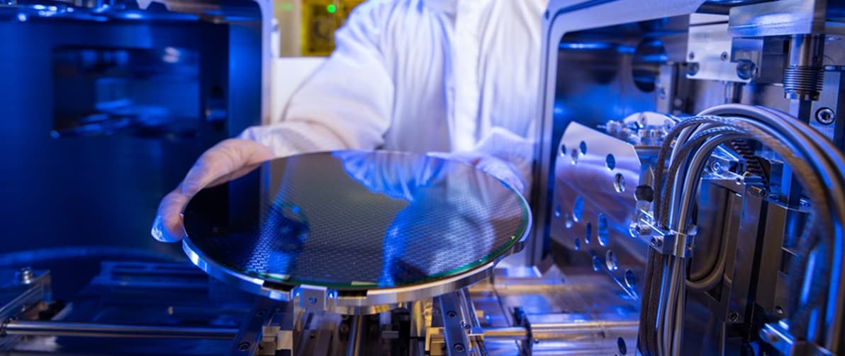
Advanced 300 mm silicon wafer manufacturing
We are expanding capacity at our 300 mm fabs in Crolles, France, and Agrate, Italy, to reinforce their scale and strengthen global competitiveness. Both facilities are engineered for the future, incorporating advanced automation and high-performance capabilities. They have flexible capacity plans with modular expansions to adapt to evolving market demands.
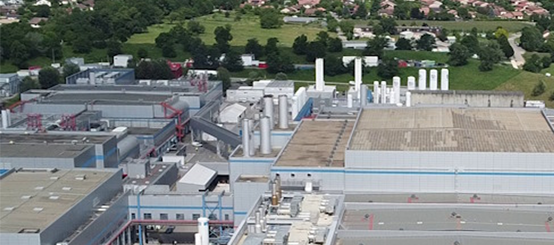
The Crolles fab strengthens its role as the core of ST’s digital products ecosystem and serves as the central R&D hub, coordinating innovation globally.
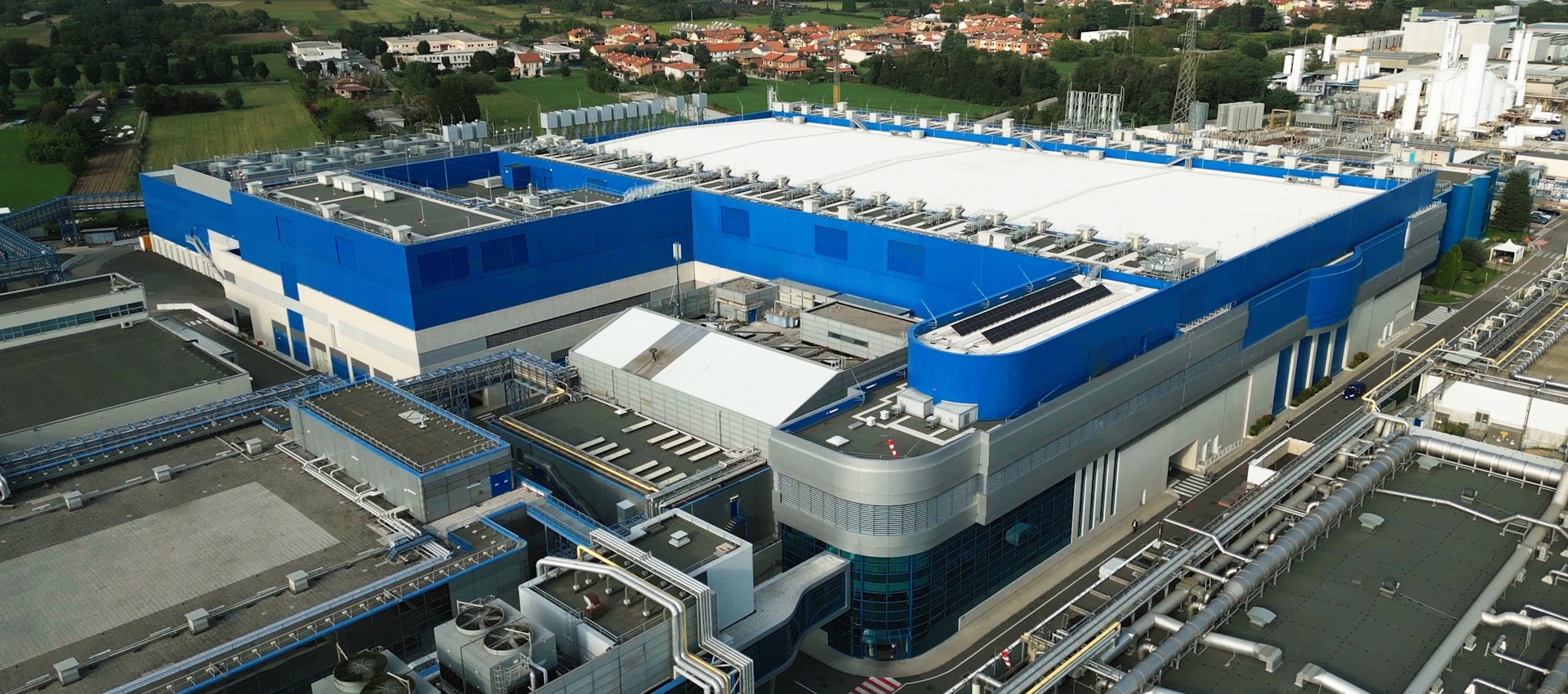
Our Agrate fab becomes the center of excellence for analog and BCD products, scaling up as ST’s flagship high-volume facility for smart power and mixed-signal technologies.
Advanced 200 mm silicon carbide manufacturing
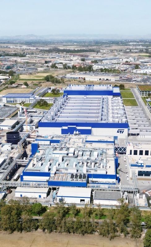
We are concentrating investment in the new Silicon Carbide Campus in Catania, Italy, as well as in our joint venture in Chongqing, China, both focused on 200 mm technology.
Catania strengthens its role as a center of excellence for power and wide-bandgap semiconductors, with 200 mm wafer production at the new Silicon Carbide Campus enhancing ST’s leadership in next-generation power technologies.
Resources supporting the current 150 mm and EWS capabilities will shift to focus on 200 mm silicon carbide and silicon power semiconductor production, including GaN-on-silicon.
Mature and legacy technologies
We are reshaping and consolidating our global 200 mm silicon capacity and upgrading our facilities with automation and the use of AI.
Ang Mo Kio (Singapore) remains focused on 200 mm silicon manufacturing and will host our consolidated global legacy 150 mm silicon capabilities.
Rousset, France, receives additional production volumes from other sites, allowing the facility to operate at full manufacturing capacity and maximize overall efficiency.
Tours, France, remains focused on its 200 mm silicon production line for selected technologies, including advanced diodes and integrated passive devices.
The Agrate 200 mm fab refocuses on MEMS technologies, supporting high‑volume MEMS sensor production with increasing levels of automation.
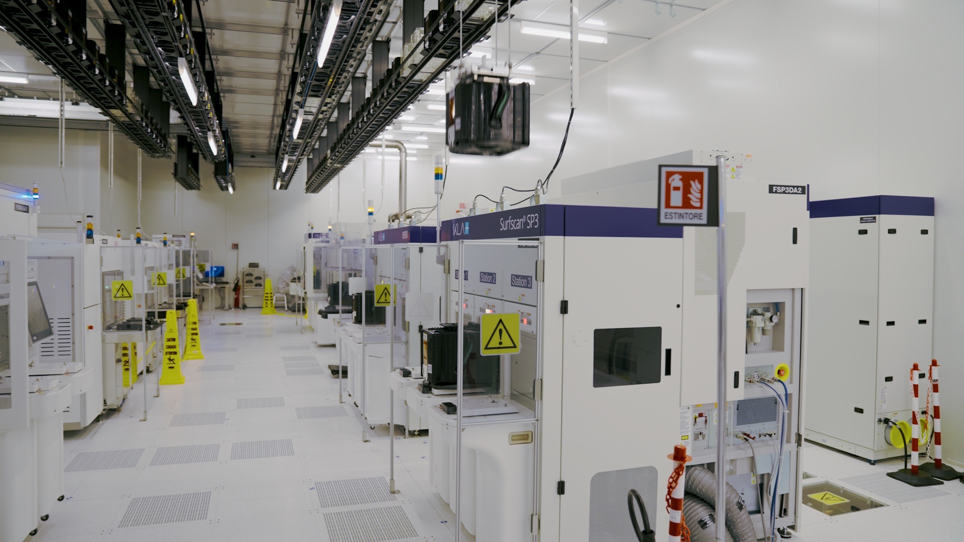
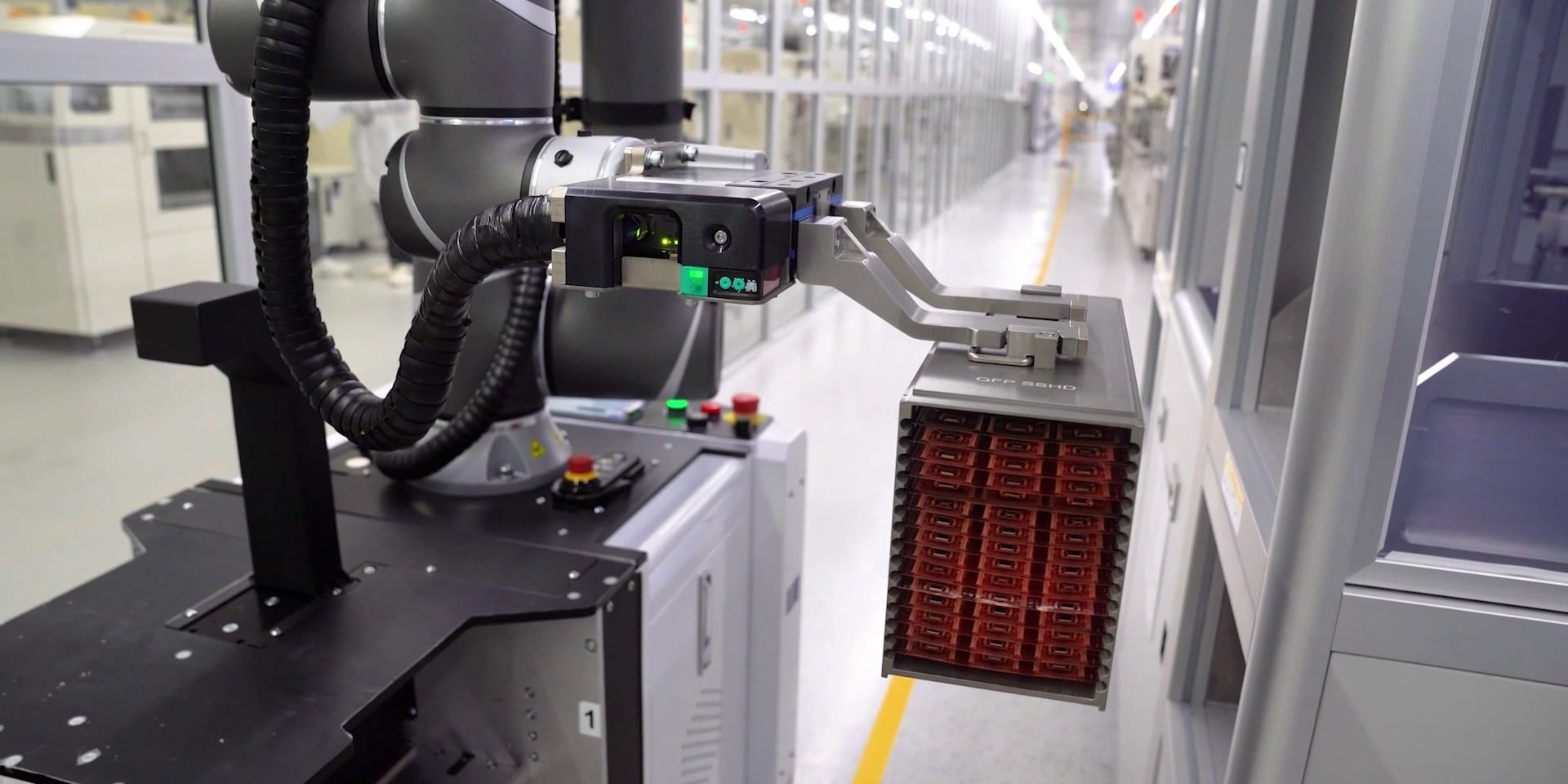
Greater automation and AI
We are continuously advancing our manufacturing capabilities and technology stack to stay ahead of market trends, embedding AI and automation throughout our R&D, manufacturing, and qualification processes.
Our 300 mm facilities in Agrate and Crolles, along with the Silicon Carbide Campus in Catania, are purpose-built to achieve industry-leading levels of automation and operational excellence.
We are also enhancing our 200 mm silicon fabs with advanced automation, driving continuous improvements in both industrial productivity and economic performance.
By prioritizing automation and AI across all operations, we are positioning ourselves for sustained, long-term success.
Next-gen packaging capabilities in Europe
Our high‑volume test and packaging fab in Kirkop, Malta, is undergoing significant upgrades, including the integration of advanced automation to support next‑generation products.
ST’s Tours site is taking on a new strategic activity with the introduction of a pilot line for panel‑level packaging, a key enabler for chiplets and an essential element of ST’s future product roadmap.
In Crolles, we are developing advanced packaging technologies that do not exist today in Europe, with a focus on next‑generation, leading‑edge solutions such as optical sensing and silicon photonics.
Developing advanced electrical wafer sorting hubs
We are establishing two advanced electrical wafer sorting (EWS) hubs, where individual chips on a wafer are electrically tested before back‑end processing and packaging. By leveraging automation and AI‑driven analytics in these EWS hubs, we are improving operational efficiency and overall product quality.
Singapore remains ST’s main EWS hub in Asia, delivering high‑volume operations and supporting the company’s global manufacturing network.
In parallel, we are creating a new advanced EWS hub in Crolles, where the 200 mm fab is being transformed to support high‑volume EWS and expand ST’s capacity in Europe.
Rousset will maintain its existing EWS manufacturing capacity to support business continuity and overall operational efficiency.
The SiC Campus in Catania will include EWS for SiC as part of its back‑end operations, together with final test and burn‑in.
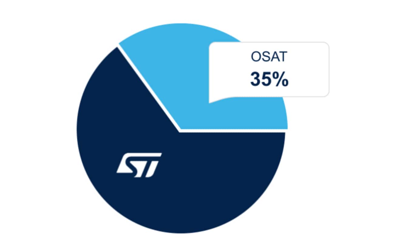
Collaboration with leading foundries and OSAT partners.
We collaborate with leading foundries and outsourced semiconductor assembly and test (OSAT) partners to enable access to selected technologies such as leading-edge digital technologies and packages to complement our portfolio.
Examples include TSMC for FinFET technology, Samsung Foundries and GlobalFoundries for the FD-SOI ecosystem, HHGrace for China supply chain, and ASE and AMKOR for advanced BGA and WLCSP packages.
Front-end
Back-end