
MEMS sensors vs. NEMS sensors: understanding the differences
In the world of sensor technology, miniaturization has been a driver of innovation. This journey led to the development of micro-electromechanical systems (MEMS), a foundational technology in modern electronics. The industry is now pushing the boundaries even further, moving from the micro-scale to the nano-scale with the advent of nano-electromechanical systems (NEMS). Both technologies integrate mechanical elements and electronics, but the transition from “micro” to “nano” represents more than just a reduction in size. It introduces a new realm of physics, materials, and potential applications.
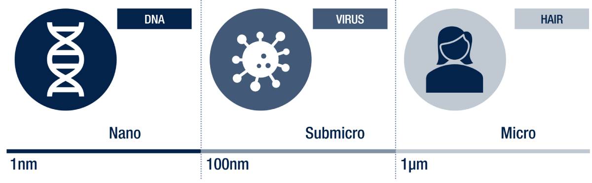
For electronic engineers, distinguishing between MEMS and NEMS is crucial to understand the current capabilities and future direction of sensor technology. This article provides a technical comparison, exploring the differences in scale, fabrication, performance, and application domains, to clarify where these technologies stand today and where they are heading.
Defining the scale: micro vs. nano
The primary difference between MEMS and NEMS lies in their characteristic dimensions.
MEMS (micro-electromechanical systems)

MEMS devices have critical structural features measured on the micrometer (μm) scale. A micrometer is one-millionth of a meter (10⁻⁶ m). The mechanical components of a MEMS device, such as the proof mass of an accelerometer or the diaphragm of a pressure sensor, typically range from a few micrometers to several hundred micrometers in size. Classical mechanics governs this scale, and fabrication uses established semiconductor processes. Our MEMS and sensors portfolio operates within this highly optimized domain.
NEMS (nano-electromechanical systems)
NEMS devices have dimensions on the nanometer (nm) scale. A nanometer is one-billionth of a meter (10⁻⁹ m), a thousand times smaller than a micrometer. At this scale, mechanical structures, such as a resonating cantilever beam, can be just a few nanometers thick or wide. This reduction in size moves technology into a physical regime where quantum mechanics and surface effects dominate the device's behavior.
Fabrication and material challenges
The shift from the micro-scale to the nano-scale introduces challenges and requires new approaches to manufacturing and material science.
MEMS fabrication
MEMS manufacturing largely relies on mature, top-down photolithography techniques inherited from the integrated circuit industry.

- Process: an ultraviolet (UV) light source projects a pattern onto a photoresist-coated silicon wafer. The exposed or unexposed resist is then removed, and the underlying silicon is etched to create the three-dimensional mechanical structures.
- Limitations:the resolution of conventional photolithography is limited by the wavelength of the light used. Advanced techniques like deep ultraviolet lithography create smaller features but are expensive and complex for features below one micrometer.
NEMS fabrication
Creating structures at the nanometer scale requires moving beyond conventional photolithography to more advanced, often bottom-up, manufacturing techniques.
- Advanced lithography: electron-beam (e-beam) lithography or extreme ultraviolet (EUV) lithography is required to achieve nanometer-scale resolution. These processes are significantly slower and more expensive than standard photolithography, making them unsuitable for mass production at present.
- New materials: silicon remains a workhorse material, but the performance of NEMS devices is often enhanced using novel materials with unique properties at the nanoscale. Two-dimensional materials like graphene and carbon nanotubes are leading candidates due to their incredible strength-to-weight ratio and electrical properties. However, integrating these new materials into a reliable manufacturing process is an ongoing research challenge.
Performance characteristics: a new frontier of sensitivity
The reduction in size from MEMS to NEMS enables higher sensitivity and resonant frequency.
| MEMS | NEMS |
|---|---|---|
| Mass | Low (micrograms) | Extremely low (femtograms) |
| Resonant frequency | High (kHz to MHz range) | Ultra-high (MHz to GHz range) |
| Sensitivity | High | Exceptionally high |
| Power consumption | Very low: typically in the microampere (µA) or milliampere (mA) range | Theoretically even lower |
| Governing physics | Primarily classical mechanics | Quantum mechanics and surface phenomena become significant |
| Surface-to-volume ratio | High: few atoms, electrons and picometer | Extremely high |
The key takeaways from this comparison are:
- Mass and sensitivity: the mass of a NEMS resonator is much smaller than a MEMS equivalent. This low mass makes it exquisitely sensitive to external stimuli. A NEMS device can detect the addition of a single molecule landing on its surface, a level of sensitivity that is unattainable with MEMS.
- Resonant frequency: NEMS resonators operate at higher frequencies (in the GHz range) due to lower mass and higher stiffness. This allows faster response times and higher quality factors (Q-factors), which translate to more stable and precise measurements.
- Surface effects:as a device size decreases, its surface-to-volume ratio increases exponentially. In NEMS, surface phenomena such as atomic-level friction and stiction become dominant and can significantly impact device performance and reliability. Managing these surface forces is a critical engineering challenge in NEMS design.
Current and future applications
The differences in maturity, cost, and performance define application domains for MEMS and NEMS.
MEMS: the technology of today
MEMS technology is mature, cost-effective, and robust, making it the dominant technology for many applications.
- Consumer electronics: MEMS accelerometers and iNEMO inertial modules are standard in every smartphone for motion sensing and image stabilization.
- Automotive: automotive sensors enable critical safety features like airbag deployment and electronic stability control.
- Industrial IoT: low-cost MEMS vibration sensors are deployed for condition monitoring, while MEMS pressure sensors monitor industrial processes. Our iNEMO inertial modules combine multiple MEMS sensors to provide integrated solutions.
NEMS: the promise of tomorrow
NEMS is a research-focused technology, with its commercial applications still on the horizon. NEMS performance promises revolutionary capabilities in highly specialized fields.

- Medical diagnostics: NEMS could enable lab-on-a-chip systems capable of detecting single viral particles or cancer biomarker proteins in blood samples, improving early-stage disease detection.
- Chemical and biological agent detection: NEMS-based resonators, functionalized with specific chemical receptors, could serve as highly selective and sensitive “electronic noses” for detecting of explosives or toxic industrial chemicals in the air.
- Ultra-high-frequency signal processing: the GHz operating frequencies of NEMS resonators make them potential candidates to replace certain electronic components in radio frequency (RF) front-end modules for next-generation wireless communication systems.
An evolutionary path in sensor technology
MEMS and NEMS represent an evolutionary relationship. NEMS is not a direct replacement for MEMS but rather a specialized extension of it. MEMS technology is reliable and cost-effective, enabling most sensor applications today. Its manufacturing processes are mature, and performance is optimized for industrial, automotive, and consumer needs.
NEMS, on the other hand, represents the research frontier. While it faces manufacturing and reliability challenges, its potential to deliver unprecedented sensitivity may revolutionize high-value applications, particularly in medical diagnostics and scientific instrumentation. For electronic engineers, MEMS remains the go-to solution for current design challenges, while NEMS offers a glimpse into the future of what is physically possible in the world of sensor technology.