Product overview
Description
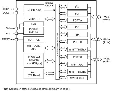
The ST72260Gx, ST72262Gx and ST72264Gx devices are members of the ST7 microcontroller family. They can be grouped as follows :
All devices are based on a common industrystandard 8-bit core, featuring an enhanced instruction set.
The ST72F260G, ST72F262G, and ST72F264G versions feature single-voltage FLASH memory with byte-by-byte In-Circuit Programming (ICP) capabilities.
Under software control, all devices can be placed in WAIT, SLOW, Active-HALT or HALT mode, reducing power consumption when the application is in idle or stand-by state.
The enhanced instruction set and addressing modes of the ST7 offer both power and flexibility to software developers, enabling the design of highly efficient and compact application code. In addition to standard 8-bit data management, all ST7 microcontrollers feature true bit manipulation, 8x8 unsigned multiplication and indirect addressing modes.
For easy reference, all parametric data is located in Section 13 on page 126.
-
All features
- 1 Analog peripheral
10-bit ADC with 6 input channels - 3 Communication Interfaces
SPI synchronous serial interface I2C multimaster interface (SMBus V1.1 Compliant) SCI asynchronous serial interface - Development Tools
Full hardware/software development package - Memories
4 K or 8 Kbytes Program memory: ROM or single voltage extended Flash (XFlash) with read-out protection, write protection, In-Circuit Programming and In-Application Programming (ICP and IAP). 10K write/erase cycles guaranteed, data retention: 20 years at 55°C. 256 bytes RAM - Interrupt Management
Nested interrupt controller 10 interrupt vectors plus TRAP and RESET 22 external interrupt lines (on 2 vectors) - Clock, Reset and Supply Management
Enhanced reset system Enhanced low voltage supply supervisor (LVD) with 3 programmable levels and auxiliary voltage detector (AVD) with interrupt capability for implementing safe power-down procedures Clock sources: crystal/ceramic resonator oscillators, internal RC oscillator and bypass for external clock PLL for 2x frequency multiplication Clock-out capability 4 Power Saving Modes: Halt, Active Halt,Wait and Slow - 4 Timers
Main Clock Controller with Real time base and Clock-out capabilities Configurable watchdog timer Two 16-bit timers with: 2 input captures, 2 output compares, external clock input on one timer, PWM and Pulse generator modes - Instruction Set
8-bit data manipulation 63 basic instructions with illegal opcode detection 17 main addressing modes 8 x 8 unsigned multiply instruction - 22 I/O Ports
22 multifunctional bidirectional I/O lines 20 alternate function lines 8 high sink outputs
- 1 Analog peripheral
Circuit Diagram
EDA Symbols, Footprints and 3D Models
STMicroelectronics - ST72260G1
Speed up your design by downloading all the EDA symbols, footprints and 3D models for your application. You have access to a large number of CAD formats to fit with your design toolchain.
Please select one model supplier :
Symbols

Footprints

3D models
All resources
| Resource title | Version | Latest update | Actions | Details | Download |
|---|
Board Manufacturing Specifications (1)
| Resource title | Version | Latest update | Actions | Options | ||
|---|---|---|---|---|---|---|
| ZIP | 1.0 | 01 Aug 2015 | 01 Aug 2015 |