R&D Digital Twin Center
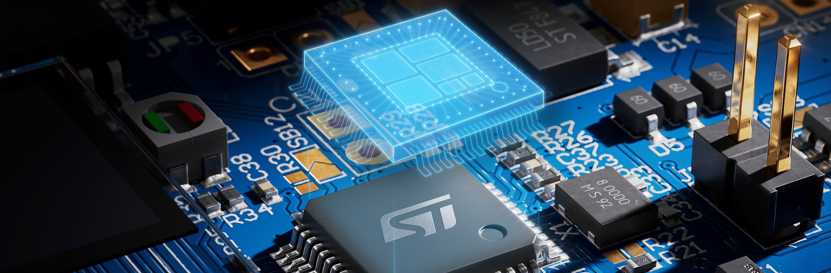
Transforming semiconductor development
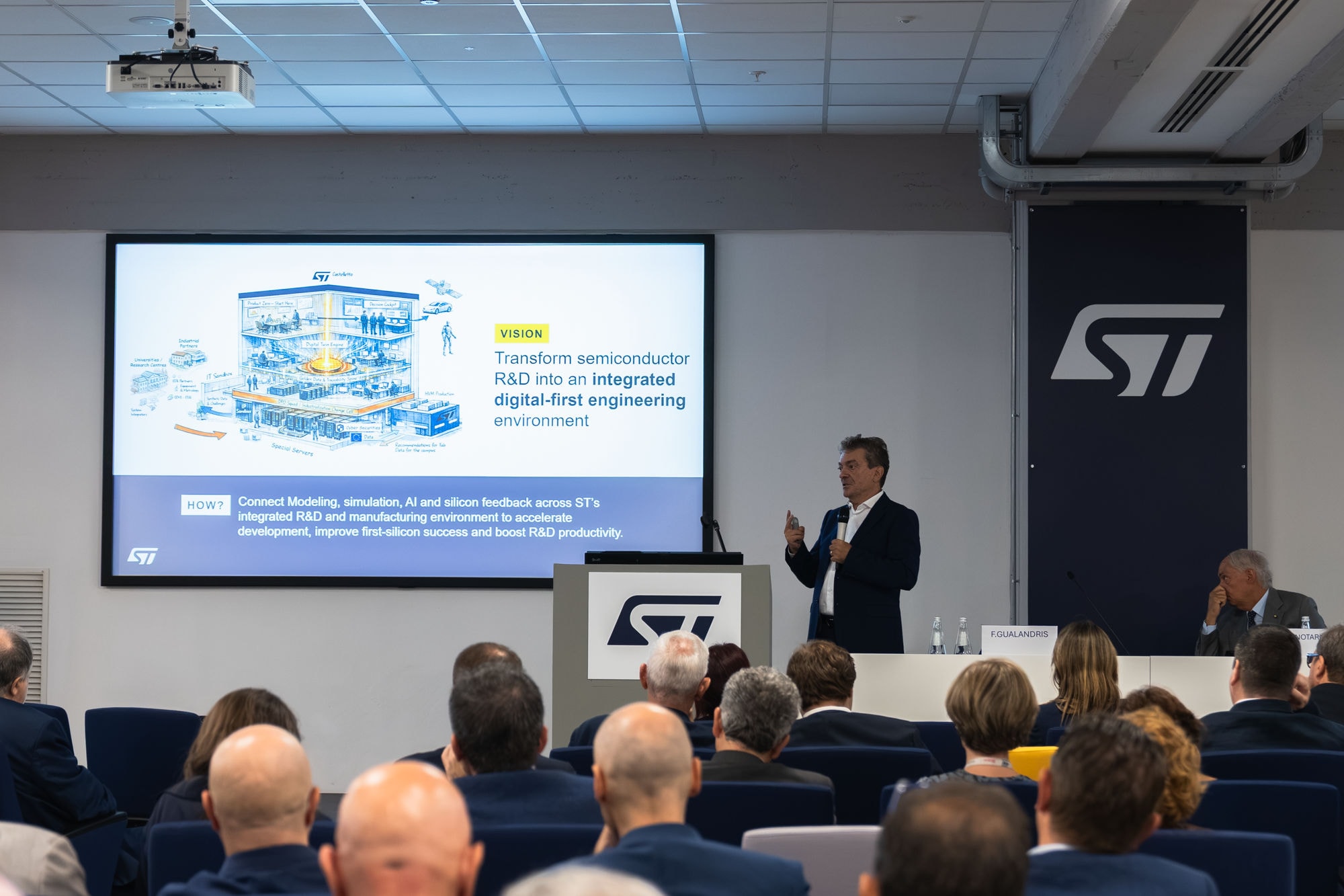
STMicroelectronics is establishing an R&D Digital Twin Center in Castelletto, Italy.
The center will strengthen semiconductor R&D, accelerate innovation and enable earlier exploration of new technologies and product concepts.
It represents an important step toward a faster, more predictive approach to research and development.
A paradigm shift in semiconductor R&D
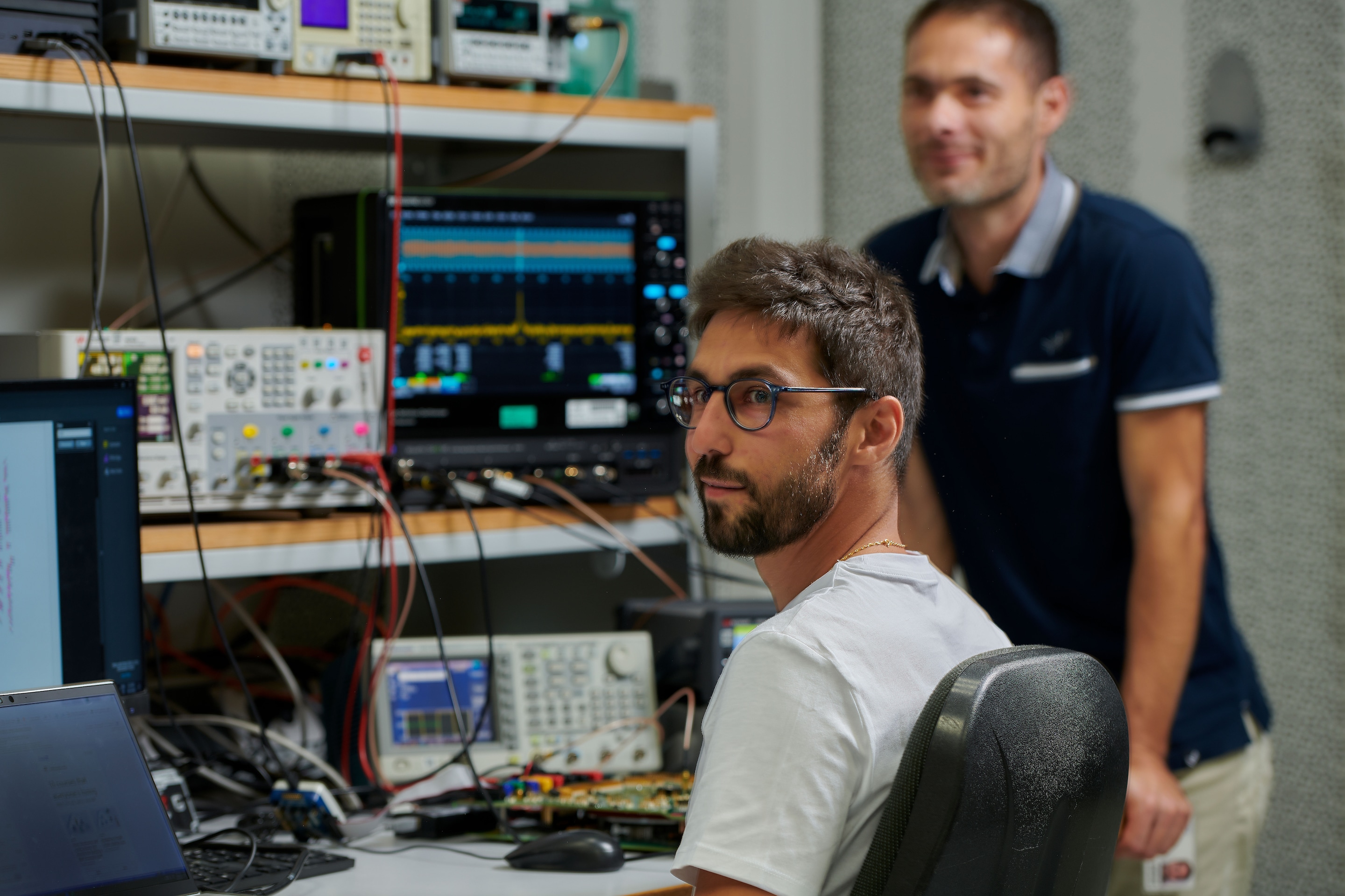
Semiconductor technologies are becoming more complex as development costs rise and timelines shorten. Much of today’s R&D learning still depends on physical silicon. Gaps between models and measured results, together with the late discovery of reliability, layout or process interactions, can create additional development loops that consume time, expertise and investment.
By connecting digital models with experimental and manufacturing data, ST’s R&D Digital Twin Center aims to reduce reliance on physical iteration. Expected benefits include shorter development cycles, stronger first-pass success, higher engineering productivity, lower costs and greater confidence before physical validation.
Castelletto connects research, industry and talent
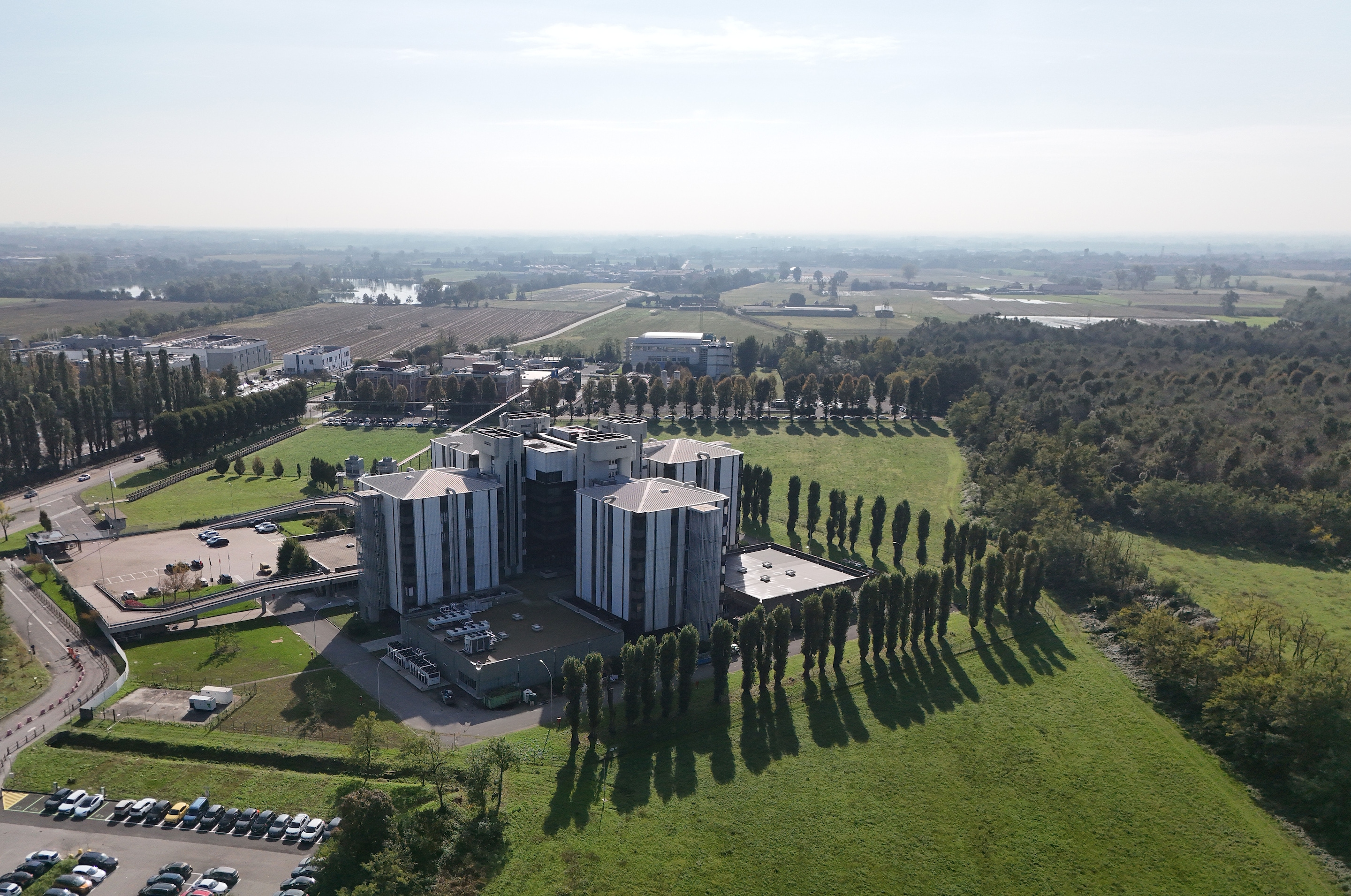
With more than 40 years of semiconductor R&D expertise, Castelletto brings together advanced research, industrial knowledge and silicon learning. Its proximity to ST’s Agrate hub and Milan’s academic and industrial ecosystem strengthens access to manufacturing capabilities, talent and research partners.
Frequently asked questions
A semiconductor Digital Twin is a continuously evolving digital representation of the interactions between semiconductor processes, devices, and circuit designs. It is continuously calibrated using data from physical experiments and silicon characterization, becoming more accurate as more real-world data is collected.
Semiconductor technologies are becoming more complex while development cycles are expected to be shorter and more cost-effective. Today, many learning cycles depend on building and testing physical silicon. ST aims to reduce these costly iterations by predicting performance and issues digitally before fabrication.
The initiative targets several measurable improvements, such as shorter technology-development cycles and lower overall devlopment costs.
These benefits should enable faster delivery of differentiated products to customers.
AI is one of the core pillars of the new R&D environment. It will work alongside physics-based models and engineering knowledge to analyze complex interactions, detect anomalies, improve predictive accuracy, and accelerate design decisions. Initial proof-of-concepts already include AI applications for silicon photonics and multivariate anomaly detection.