GaN
Gallium Nitride

GaN: the future of power electronics
ST has gained significant experience in wide bandgap (WBG) materials through silicon carbide (SiC) MOSFETs and SiC diodes. We are now taking the next step in smart power integration with the development of gallium nitride grown on silicon substrates. The very high electron mobility of GaN material allows devices with very low on-resistance and exceptionally high switching frequencies, which are key advantages in the design of next generation power systems, especially those for electric vehicles and renewable energy applications.
GaN-based high-electron-mobility transistors (HEMT) can therefore deliver major gains in terms of efficiency and power density in circuit topologies involving high frequency operation and low on-state resistance. This is especially true in the lower voltage and lower power application ranges involving significantly higher switching frequencies.
Helping you build better power solutions
Ideal for high frequency operation with low switching losses.

Suitable for many power applications
ST GaN products will be targeting a wide variety of applications, such as power supplies and adaptors (PC, portable electronics, wall USB chargers, wireless chargers, etc.), power factor correction (PFC), and DC/DC converters. Regarding the automotive sector, GaN devices are particularly well suited for high-efficiency EV on-board chargers and mild-hybrid DC-DC converters at low voltage.
ST GaN technology is also highly suitable for integrated solutions such as the STi²GaN. New packaging concepts such as the embedded 2SPAK and PowerFLAT packages are also an integral part of GaN development, as they help manage the exceptionally high switching frequencies with packages that feature very low internal parasitic inductance.
Benefits of GaN power devices
Benefits of GaN power devices
Thanks to their superior performance GaN HEMTs help designers achieve higher conversion efficiency, smaller form factors, and new levels of power density.
Low on resistance (RDS(ON)) due to high electron mobility of the two-dimensional electron gas (2DEG)
High breakdown voltage linked to large bandgap (3.4 eV) and high critical electric field
Low capacitances & low gate charge
Higher operation frequency
CMOS-compatible lateral device
Bidirectional switching diodes Advantageous in certain circuit topologies such as OBC
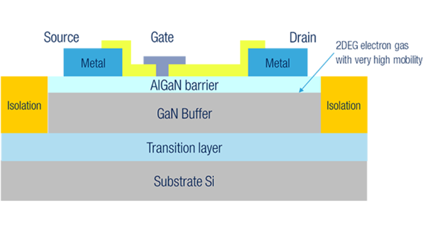
AlGaN/GaN HEMT structure
What exactly is gallium nitride (GaN)?
Gallium Nitride (GaN) belongs to the family of wide bandgap (WBG) materials. It is a binary compound whose molecule is formed from one atom of Gallium (III-group, Z=31) and one of Nitrogen (V-group, Z=7) with a basic hexagonal (wurtzite) structure.
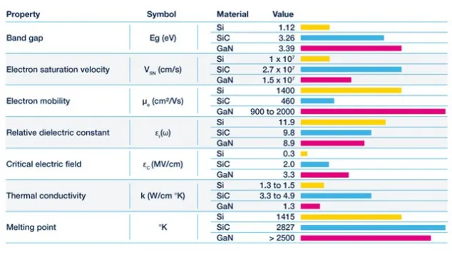
Comparison of the electrical and thermal properties of silicon, silicon carbide, and gallium nitride
Learn more about Gallium Nitride Read our whitepapers
Benefits of using ST's wide bandgap technology
Get a true feedback about which application types and conditions it makes sense to use SiC MOSFETs rather than traditional silicon devices in terms of performance and cost-effectiveness.