Silicon photonics

Scaling cloud AI with high-speed optical connectivity
How to meet rising computing demands in data centers
As AI infrastructure scales, data must move faster and with greater efficiency. Generative AI, agentic AI, and large language models are pushing data center infrastructure to an inflection point, where bandwidth, latency, power consumption, and thermal constraints are becoming limiting factors for conventional electrical interconnects.
The next generation of AI data centers are shifting high-bandwidth interconnects from electrical signaling to optics, with silicon photonics providing the reach, bandwidth density and lower energy per bit needed to scale. Silicon photonics is projected to grow from 43 to 76% of AI cluster optical technology between 2024 and 2030 (LightCounting).
Our PIC100 silicon photonics platform supports this transition by enabling high-speed optical connectivity for AI and cloud infrastructure.
About PIC platform
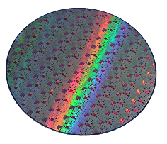
PIC100 is an advanced silicon photonics platform designed for modulation, encoding, and data tranmission at scale.
Already in volume production, PIC100 provides a proven foundation supporting speeds up to 100 Gbaud and optical modules from 800 Gb/s to 1.6 Tb/s.
The next generation, PIC200, targeting 200 Gbaud is under development.

PIC100 is produced at ST 300 mm foundry in Crolles, France. With production capacity set to grow by more than fourfold by 2027, we give hyperscalers and makers of optical transceivers a scalable source of silicon photonics capacity. As an integrated device manufacturer, we produce PIC100 in-house to support long-term supply planning, including our multi-year strategic collaboration with AWS.

Network connectivity inside AI data centers: scale-X
AI infrastructure extends across three connectivity layers: scale-up, which tightly couples GPUs and accelerators within a server or rack; scale-out, which connects servers and racks across an AI cluster; and scale-across, which links separate AI clusters across a campus, metro area, or multiple data centers.
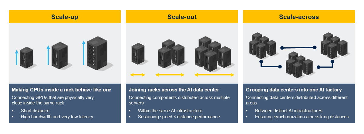
- Scale-up networks connect GPUs or other accelerators, memory, and switching fabric within a server or rack typically over distances from one to five meters. Their role is to make distributed resources behave as much as possible like a single high-performance system. Scale-up networks require extremely high bandwidth, very low latency, high I/O density, and low energy consumption per transmitted bit (pJ/bit). As accelerator counts and bandwidth demands grow, electrical I/O becomes a performance and physical area bottleneck. Near-package optics (NPO) and co-packaged optics (CPO) can help overcome these constraints by delivering higher bandwidth density with better energy efficiency in a compact form.
- Scale-out networks connect servers and racks across an AI cluster, spanning from ten to around hundred meters. They carry the high-volume east-west traffic required for distributed training and inference, commonly using Ethernet-based fabrics. Scale-out prioritizes modularity, serviceability, and reach, and typically uses pluggable optical transceivers to connect switches and servers across data halls or between buildings.
- Beyond scale-out, scale-across networks extend connectivity past a single cluster or site, ranging from several to hundreds of kilometers. They connect separate AI clusters across multiple data centers, extending the network to form a larger logical compute domain. These networks are used when power, space, or capacity constraints require workloads to be distributed across physically distant locations. They typically rely on long-reach optical interconnects to preserve manageable latency and operational flexibility.
The growing role of optical fiber in cloud interconnects
Modern cloud and AI factories connect thousands of GPUs, making network performance as important as compute performance.
Copper is currently effective for short in-rack links. But at higher speeds and longer distances, signal loss, power use, and heat constrain electrical interconnects.
Hyperscalers are therefore expanding fiber-based optical links across AI clusters and data centers. Optical connectivity supports higher-bandwidth scale-out networks, including 800 Gb/s and 1.6 Tb/s deployments.
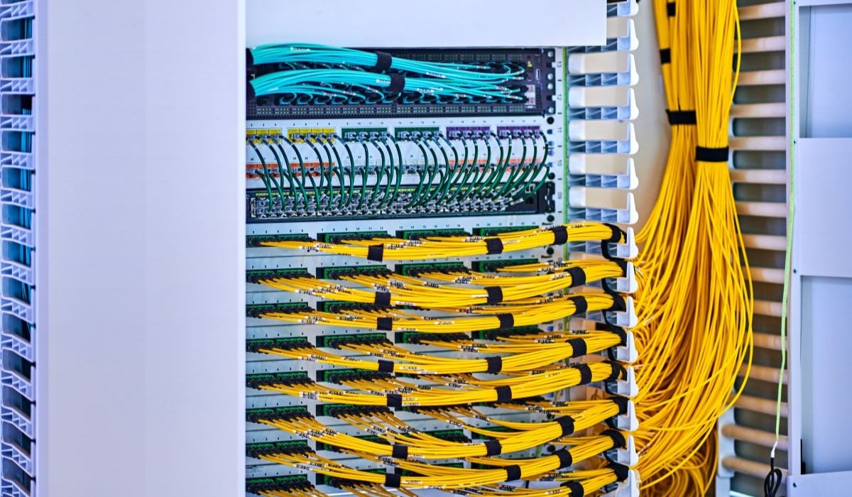
ST technology portfolio for optical engines
GPUs, switches, and servers process and move data as electrical signals. Pluggable optical transceivers convert those signals into light for transmission over optical fiber, then convert them back into electrical signals at the receiving end.
These modules form the link between electronic compute infrastructure and high-speed optical networks. As bandwidth, reach, and power density requirements continue to grow, the optical engine plays a critical role in meeting system-level performance demands.
ST supplies multiple technologies used within the optical engine: silicon photonics for optical functions, BiCMOS for electrical signal conditioning, and microcontrollers for control and operation. This broad technology portfolio helps transceiver manufacturers streamline integration.
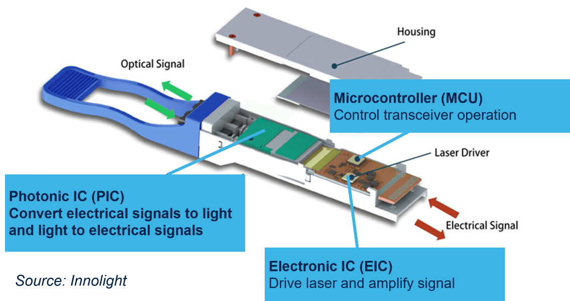
The photonic integrated circuit (PIC) is the optical core of the module. It integrates functions such as optical modulation, waveguides and photodetection, enabling conversion between electrical data and modulated light. ST proprietary PIC100 silicon photonics platform is designed for 200 Gbps-per-lane PAM4 operation, supporting next-generation 800 Gb/s and 1.6 Tb/s pluggable transceivers.
ST proprietary silicon-germanium BiCMOS B55X technology provides the high-speed electronic interface to the PIC, including laser drivers on the transmit side and transimpedance amplifiers on the receive side. It is engineered to provide the bandwidth, signal integrity and power efficiency needed for very-high-speed optical links. Its excellent linearity is well suited for linear pluggable optics, enabling architectures that reduce the need for DSP and therefore improve power efficiency.
STM32 microcontrollers, such as the STM32H5, provide module configuration, monitoring, diagnostics, and system management, supported by the extensive STM32 ecosystem of software tools, development environments, and long-term availability.
Today: pluggable optics
Pluggable optics support 100 Gb/s and 400 Gb/s and are scaling toward 800 Gb/s and 1.6 Tb/s. They offer strong modularity and flexibility through front-panel modules and are widely used for scale-out connectivity.
Phase 2: near-packaged optics (NPO)
NPOs move the optical engine closer to the processor on the host PCB. This shortens the electrical path, improves bandwidth density and energy efficiency, and better addresses the needs of scale-up newtorks.
Phase 3: co-packaged optics (CPO)
CPOs integrate the optical engine on the same substrate as the processor. Using advanced packaging such as through-silicon vias (TSVs), this approach targets even higher power efficiency and data density, enabling 3.2 Tb/s and beyond for the most demanding scale-up and high density architectures.
The future of optical connectivity
As data center traffic continues to scale, the adoption of optical interconnects is growing and architectures are evolving to address three critical requirements: the need for more bandwidth, for greater power efficiency, and for higher integration density.
From pluggable modules to near-packaged and co-package optics, each steps shortens the electrical path and brings optical data transmission closer to the processor.
The future of optical connectivity
As data center traffic continues to scale, the adoption of optical interconnects is growing and architectures are evolving to address three critical requirements: the need for more bandwidth, for greater power efficiency, and for higher integration density.
From pluggable modules to near-packaged and co-package optics, each steps shortens the electrical path and brings optical data transmission closer to the processor.
Today: pluggable optics
Pluggable optics support 100 Gb/s and 400 Gb/s and are scaling toward 800 Gb/s and 1.6 Tb/s. They offer strong modularity and flexibility through front-panel modules and are widely used for scale-out connectivity.
Phase 2: near-packaged optics (NPO)
NPOs move the optical engine closer to the processor on the host PCB. This shortens the electrical path, improves bandwidth density and energy efficiency, and better addresses the needs of scale-up newtorks.
Phase 3: co-packaged optics (CPO)
CPOs integrate the optical engine on the same substrate as the processor. Using advanced packaging such as through-silicon vias (TSVs), this approach targets even higher power efficiency and data density, enabling 3.2 Tb/s and beyond for the most demanding scale-up and high density architectures.
Meet ST at events

Sep 20-24, Spain
The latest ST innovation in silicon photonics and AI-driven data center infrastructure shaping cloud connectivity.

Nov 3-4, The Netherlands
Luca Verre, Head of Strategy, Microcontrollers, Digital ICs & RF products Group, will speak at the event.

March 7-11, USA
Explore ST's latest advances in silicon photonics and AI-driven data center infrastructure for next-generation cloud connectivity.
Related knowledge
| The winning portfolio for AI optical interconnects | |
| Driving the future of AI data centers | |
| ST to drive EU-funded STARLight project | |
| EETimes: AI data centers push silicon photonics toward 300-mm scale | |
| ICs & Semiconductors: silicon photonics scales up | |
| Datacentre solutions: PIC100 platform enters high volume production |