Product overview
Description
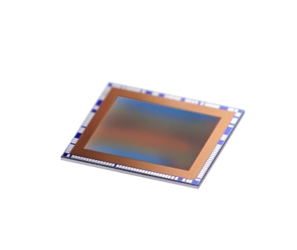
The VD55H1 is a low-noise, low-power, 672 x 804 pixel (0.54 Mpix), indirect Time-of-Flight (iToF) sensor die manufactured on advanced backside-illuminated, stacked wafer technology. Combined with a 940 nm illumination system, it enables building a small form-factor 3D camera producing a high-definition depth map with typical ranging distance up to 5 meters in full resolution, and beyond 5 meters with patterned illumination. With a unique ability to operate at 200 MHz modulation frequency and more than 85% demodulation contrast, the sensor can produce depth precision twice as good as typical 100 MHz modulated sensors, while multifrequency operation provides long distance ranging. The low-power 4.6 µm pixel enables state-of-the-art power consumption, with average sensor power down to 80 mW in some modes.
The VD55H1 outputs 12-bit RAW digital video data over a MIPI CSI-2 quad lane or dual lane interface clocked at 1.5 GHz. The sensor frame rate can reach 60 fps in full resolution and 120 fps in analog binning 2x2. ST has developed a proprietary software image signal processor (ISP) to convert RAW data into depth map, amplitude map, confidence map and offset map. Android formats like DEPTH16 and depth point cloud are also supported.
The device is fully configurable through the I2C serial interface. It features a 200 MHz low-voltage differential signaling (LVDS) and a 10 MHz, 3-wire SPI interface to control the laser driver with high flexibility. The sensor is optimized for low EMI/EMC, multidevice immunity, and easy calibration procedure.
The sensor die size is 4.5 x 4.9 mm and the product is delivered in the form of reconstructed wafers.
-
All features
- Ultra-compact 0.54 Mpix iToF sensor die
- 672 x 804 indirect Time-of-Flight (iToF) sensor die (0.54 Mpixel)
- 4.6 μm backside illuminated fast photodiode pixel, 1/4’’ optical format
- 4.5 mm x 4.9 mm die manufactured on advanced 40 nm stacked wafer technology
- Enabling low-power, high precision depth map
- Pixel with >85% demodulation contrast at 200 MHz modulation frequency
- Low noise charge domain pixel (kTC free) < 5e-
- Multifrequency supported (up to three frequencies)
- Average sensor power consumption down to 80 mW
- Smart iToF modulation, no need for wiggling error calibration
- Multi-user interferences reduction
- Optimized for low EMI/EMC
- Easy integration for 3D camera
- Raw data output on MIPI CSI2 interface at 1.5 GHz (quad or dual lane)
- 10/12-bit configurable ADC resolution
- Sensor raw output up to 120 fps (depth-level frame rate)
- Sensor control: Fast mode+ I2C slave interface (up to 1 MHz)
- Laser driver interface: LVDS and 3-wire SPI
- Software ISP for depth reconstruction available
- Ultra-compact 0.54 Mpix iToF sensor die
You might also like...
Recommended for you
EDA Symbols, Footprints and 3D Models
Quality and Reliability
| Part Number | Marketing Status | Package | Grade | RoHS Compliance Grade | Longevity Commitment | Longevity Starting Date | Material Declaration** |
|---|---|---|---|---|---|---|---|
| VD55H1CCA0/RW | Active Product is in volume production. | GOOD DIE | Industrial | N/A | - | - |
(**) The Material Declaration forms available on st.com may be generic documents based on the most commonly used package within a package family. For this reason, they may not be 100% accurate for a specific device. Please contact our sales support for information on specific devices.

You’re now leaving st.com and will be re-directed to our Partner’s website.
For the latest innovations and solutions from ST, sign up for our newsletters.
Sample & Buy

| Part Number | Marketing Status | Budgetary Price (US$)*/Qty | Order from ST | Order from distributors | Package | Packing Type | RoHS | Country of Origin | ECCN (US) | ECCN (EU) | Operating temperature (°C) | Operating Temperature (°C) (max) | Operating Range Distance (m) (max) | Package size (mm) | ||
|---|---|---|---|---|---|---|---|---|---|---|---|---|---|---|---|---|
| min | max | |||||||||||||||
| VD55H1CCA0/RW | | | distributors No availability of distributors reported, please contact our sales office |
|
| |||||||||||

VD55H1CCA0/RW Active
(*) Suggested Resale Price (USD) per defined quantity for BUDGETARY USE ONLY. For quotes, prices in local currency, please contact your local ST Sales Office or our Distributors


