PCM
Phase-change memory


Phase-change memory (PCM) technology
The integration of conventional floating gate embedded Non-Volatile Memories (eNVM) represents a significant technical challenge in advanced CMOS technologies. To solve this, NVM technologies based on exotic materials using radically different mechanisms than those of flash memory have come to the fore. Among these technologies is phase-change memory (PCM).
The fundamental mechanism for PCM was invented in the 1960s by Stanford Robert Ovshinsky. ST holds a license to the patents that resulted from that original development and has built onto that ground-breaking work.
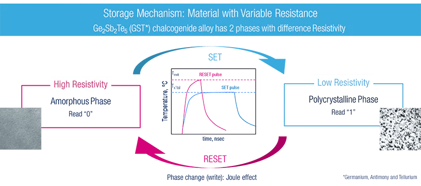
PCM is made using a Germanium Antimony Tellurium (GST) alloy. It takes advantage of rapid heat-controlled changes in the material’s physical property between amorphous and crystalline states. These states, which correspond to logic 0 and 1, are electrically differentiated by high resistance in the amorphous state (logic 0) and low resistance in the crystalline state (Logic 1). PCM, which reads and writes at low voltage, offers several substantial advantages over Flash and other embedded memory technologies.
PCM technology architecture
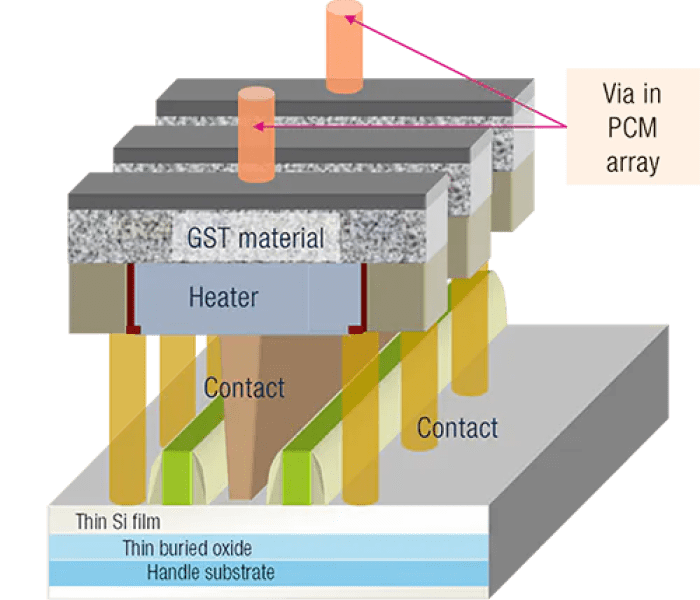
A cross section of the embedded-PCM bitcell integrated in FD-SOI technology shows the heater that quickly flips storage cells between crystalline and amorphous states.
Combining technologies
ST has pioneered the combination of FD-SOI with PCM technology as an innovative solution for demanding embedded processing applications. This combination offers significant advantages vs bulk CMOS with conventional floating gate eNVM. It improves performance and power consumption while allowing larger memory sizes and higher levels of integration.
Advantages vs bulk technology
Many of today’s advanced microcontrollers use 40 nm bulk eNVM Technology. 18 nm FD-SOI with ePCM delivers significant improvements:
- >50% better performance-to-power ratio
- 2.5x smaller non-volatile memory
- 3x higher digital density
- 3 dB improvement in RF noise figure
This will benefit a broad range of microcontrollers, from high performance to ultralow power to wireless devices.
Memory advantages
PCM allows significantly higher memory density than flash-based eNVM. With single-bit alterability, PCM technology also delivers significantly better write and comparable read performance. ST’s implementation benefits from patented technology that supports high-temperature data retention, including during solder reflow, so firmware can be uploaded before soldering.
Robust & reliable
ST’s PCM technology has been developed and tested to deliver high-temperature operation, radiation hardening, and data retention. PCM achieves automotive requirements for AEC-Q100 Grade 0 with an operating temperature up to +165°C.
3V capability at 18 nm
ST’s PCM + FD-SOI technology is capable of 3 V operation down to 18 nm. This is key for analog features such as power management and digital / analog converters. It is the only sub-20 nm technology supporting this capability.
PCM + FD-SOI applications
Ever more demanding applications are pushing the limits of MCU architectures due to their need for more processing power, lower power consumption, and larger memory sizes. One of the most challenging demands is for larger embedded memories.
PCM presents a solution to these chip- and system-level challenges, while meeting the demanding requirement for automotive and industrial. In addition, ST’s technology assures data retention through high-temperature soldering reflow processes and immunity to radiation.
ST has already brought combined PCM and FD-SOI technologies to automotive and aerospace applications in a 28 nm process. The latest process combining these technologies in 18 nm is bringing the benefits to developers of industrial applications starting with our next-generation STM32 microcontrollers, the STM32V8.